■ Introduction
In recent years, image processing from multiple cameras and AI inference have become commonplace in automotive ECUs, resulting in a rapid increase in the amount of data handled by SoCs. At the same time, ECUs must also be able to withstand a wide temperature range of -40°C to 125°C, due to the strict constraints of onboard POWER SUPPLIES. Not only is the onboard POWER SUPPLIES subject to large voltage fluctuations, but the amount of power available to the entire vehicle is also limited. Under these conditions, ECUs must maintain stable operation while enduring limited power and an unstable POWER SUPPLIES environment. Therefore, managing power consumption and heat generation has become a key design issue in the development of automotive ECUs.
In particular, memory, which exchanges large amounts of data with SoCs, has a significant impact on power consumption and heat generation, making it increasingly important for improving processing performance. LPDDR memory, which was developed for smartphones, is increasingly being adopted in automotive ECUs due to its ability to combine low power consumption with high data rates. This article provides a step-by-step explanation of memory basics, the properties of DYNAMIC RAMS, and the differences between LPDDR4 and LPDDR5, making it easy to understand even for beginners.
1. What is Memory?
Memory is broadly divided into volatile and non-volatile types. Volatile memory loses its contents when POWER SUPPLIES is turned off, while non-volatile memory retains its data even after POWER SUPPLIES is turned off.
Volatile memory has high-speed read and write speeds and is used to store data handled by the processor in real time, while non-volatile memory is used for saving software and storing initialization information, with the roles of memory clearly divided according to their use.
2. What is DYNAMIC RAMS?
DYNAMIC RAMS (Dynamic RAM) is a representative volatile memory with a relatively simple structure that allows for easy storage capacity. It is used as a working area in many devices, including PCs, smartphones, and automotive devices. In automotive SoCs, there is an increasing need for processing that requires high-bandwidth data transfer, such as image processing and AI inference, and the performance of DYNAMIC RAMS directly affects the performance of the entire system.
DYNAMIC RAMS uses tiny CAPACITORS to store electrical charge to retain data, but this charge naturally decreases over time, so the data must be periodically rewritten, a process known as refreshing.
As temperature rises, the rate at which charge is lost also increases, requiring that refresh intervals be shorter. This refresh operation reduces the time that memory can actually use for reading and writing, thereby affecting latency. In addition, increasing the number of refresh operations increases the number of times the internal circuits operate, which also leads to increased power consumption. For this reason, in applications where high temperature operation is required, such as in-vehicle applications, DYNAMIC RAMS performance is easily affected by temperature increases.
DYNAMIC RAMS operates when the controller issues commands to perform various operations such as read, write, and refresh via signal lines called CA (Command/Address). The CA signal tells DYNAMIC RAMS which operation to perform and which address (bank, row, column) to perform it on.
These commands and addresses are synchronized with the CK (Clock) signal input to DYNAMIC RAMS. DYNAMIC RAMS is essentially a synchronous memory, and the timing of internal operations is determined by sampling the CA signal based on the rising (or falling) edge of CK.
Meanwhile, when actually reading and writing data, a data bus called the DQ (Data) signal is used. During a write operation, the controller outputs write data to the DQ signal, which is received by DYNAMIC RAMS. During a read operation, DYNAMIC RAMS drives the DQ signal to output data, which is received by the controller. At this time, the valid sampling timing of the DQ signal is strictly regulated relative to the clock.
In this way, the basic operation of DYNAMIC RAMS is structured by a division of roles: the CA signal specifies "what to do," the clock determines "when to do it," and the DQ signal transfers "the actual data."
Understanding the relationship between CA, CK, and DQ is also important for understanding signals such as WCK (Write Clock) and RDQS (Read Data Strobe) in LPDDR5, which will be introduced later, and is the foundation for learning the principles of DYNAMIC RAMS operation.
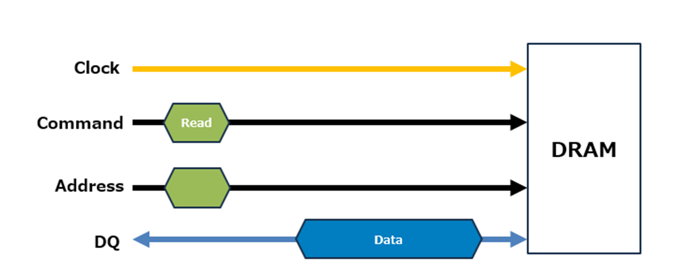
Relationship between Read command and data
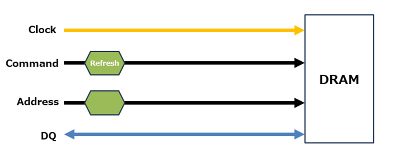
Refresh Command
In addition to LPDDR, there are various types of DYNAMIC RAMS, including DDR for PCs, GDDR for GPUs, and HBM, which achieves high bandwidth through 3D stacking. Of these, LPDDR types are the leading candidates for automotive applications due to their excellent balance of performance and power consumption, and their evolution with each generation directly leads to improved performance of automotive systems. The main types of DYNAMIC RAMS are summarized below.
Table 1. Main types of DYNAMIC RAMS
| Types | Features | Purpose |
|---|---|---|
| S-DYNAMIC RAMS | Clock synchronous type. High speed because it operates in sync with the CPU. | Old PCs and embedded devices |
| DDR S DYNAMIC RAMS | Data transfer occurs on both the rising and falling edges of the clock. | General PC or laptop |
| LPDDR | Low-power DDR for mobile devices. | Smartphones and TABLETS |
| GDDR | High-speed memory optimized for GPUs. | Graphics card |
| HBM | High speed, high bandwidth, space saving. 3D stacked structure. | For high-end GPUs and AI processing |
3. What is LPDDR?
LPDDR (Low-Power DDR), as its name suggests, is DYNAMIC RAMS designed with an emphasis on low power consumption, and has evolved along with the spread of smartphones. It features I/O circuits that operate at low voltage and a sleep mode that allows for precise power control, giving it higher performance per watt than standard DDR and reducing heat generation even when performing the same processing.
With each generation of LPDDR, the data transfer speed (data rate) has improved significantly. Mb/s (Megabit per second), which represents the data rate, is a number that indicates how many times data can be transferred per second. With each generation, the speed has increased, from a maximum of 4266 Mb/s for LPDDR4, 6400 Mb/s for LPDDR5, and 8533 Mb/s for LPDDR5X. This increase in speed makes it possible to handle large amounts of data, such as data from high-resolution cameras and advanced AI inference.
Table 2 Comparison of LPDDR standards by generation
| Year of publication | name | JEDEC standard | Data rate |
|---|---|---|---|
| 2006 | LPDDR | JESD209 | ~533 Mb/s |
| 2009 | LPDDR2 | JESD209-2 | ~1066 Mb/s |
| 2012 | LPDDR3 | JESD209-3 | ~2133 Mb/s |
| 2014 | LPDDR4 | JESD209-4 | ~4266 Mb/s |
| 2017 | LPDDR4X | JESD209-4 revised | ~4266 Mb/s |
| 2019 | LPDDR5 | JESD209-5 | ~6400 Mb/s |
| 2021 | LPDDR5X | JESD209-5 revised | ~8533 Mb/s |
| Reference | LPDDR6 | JESD209-6 | 10667 Mb/s and up |
4. Evolution from LPDDR4 to LPDDR5
The key features of LPDDR5 can be summed up in one sentence: "Memory with an overall redesigned structure that operates faster and with less power." For example, the CA bus used to send commands has been changed from the SDR*1 format used in LPDDR4 to the DDR*2 format, which increases the number of instructions that can be transferred in the same amount of time and reduces command latency at high transfer rates. This results in improved efficiency and reduced overhead during high-speed operation.
The key to achieving this speed increase is a mechanism that accurately synchronizes the timing of data transfers.
In the conventional LPDDR4, DQS*3 was used for both reading and writing, but in LPDDR5, these roles have been separated, with WCK*3 used for writing and RDQS*3 used for reading. By clearly separating the operations of the transmitting and receiving sides, the device is less susceptible to the effects of wiring delays and jitter, enabling stable timing synchronization even at high data rates. Since even minute skew can be fatal, especially in high-speed areas, this structural innovation is an important point in achieving both signal integrity and stable operation.
*1 SDR (Single Data Rate): A method of transferring data once per rising edge of a reference signal.
*2 DDR (Double Data Rate): A method of transferring data on both the rising and falling edges of a reference signal.
*3 DQS/WCK/RDQS: DQ transfer signals (data strobe signals)

DQS Synchronization for LPDDR4

WCK/RDQS separation for LPDDR5
In addition, POWER SUPPLIES structure has been streamlined in LPDDR5, with POWER SUPPLIES such as VDD1/VDD2H/VDD2L/VDDQ being divided according to their intended use.
-
VDD1: Approximately 1.8V. POWER SUPPLIES operates the analog and peripheral circuits inside DYNAMIC RAMS, such as reference voltage generation and control LOGIC.
-
VDD2H: Approximately 1.05V. This is the core POWER SUPPLIES used for high-speed operation when a high data rate is required.
-
VDD2L: Approximately 0.9V. This is the core POWER SUPPLIES for low-speed, power-saving operation. The internal circuitry automatically switches over depending on the operating frequency, reducing power consumption.
-
VDDQ: Approximately 0.5V. This is POWER SUPPLIES for data input/output. It operates at an extremely low voltage, allowing for significant reductions in I/O power. The voltage drops from 1.1V to 0.50V from LPDDR4 to LPDDR5, significantly reducing the power required for data input/output. This difference is particularly significant in environments such as automotive, where thermal design is strict and there is a clear upper limit on power consumption.
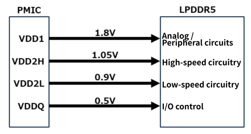
LPDDR5 POWER SUPPLIES separation
We have summarized the main differences between the representative LPDDR4 and LPDDR5.
Table 3 LPDDR4 and LPDDR5
| LPDDR4 | LPDDR5 | |
|---|---|---|
| package | 200 ball | 315 balls / 441 balls |
| Bus Width | x32 | x32 / x64 |
| Voltage | VDD1 = 1.8V VDD2 = 1.1V VDDQ = 1.1V | VDD1 = 1.8V VDD2H = 1.05V VDD2L = 0.9V / 1.05V VDDQ = 0.50V / 0.45V / 0.35V |
| Clock frequency | ~2133MHz | ~800MHz |
| CA Bus | SDR: ~2133Mb/s | DDR: ~1600Mb/s |
| Data Strobe | DQS: ~2133MHz | WCK (for Write): ~3200MHz RDQS (for Read): ~3200MHz |
| Data rate | ~4266Mb/s | ~6400Mb/s |
5. Understanding data entry specifications (Mask method)
In LPDDR, the range within which the memory can recognize the received signal as "correct data" is defined in terms of "at what timing and voltage it can be read." This is the data input tolerance range (input margin).
Previous methods evaluated data based solely on time, such as the setup time (tDS) and hold time (tDH) required to read the data. However, starting with LPDDR4, a "Mask method" was introduced that checks both time and voltage simultaneously to more accurately evaluate waveforms. This allows for more effective stability evaluation, taking into account fluctuations in voltage levels and the effects of noise.
The Mask method defines the range in which data reading is stable as a rectangular frame of "time x voltage." It is similar to the eye pattern seen on an oscilloscope. An eye pattern is a diagram in which waveforms overlap to form an "eye." The larger this "eye," the easier it is to read the data, and the smaller it is, the more likely errors will occur. The Mask method works by considering that as long as the waveform (DQ) fits within the mask frame, it's OK, which is the same concept as the size of the eye in an eye pattern.
With LPDDR5, the data rate has been further improved, narrowing the input margin tolerance "window." This means that even slight variations in timing or voltage can easily lead to errors. Therefore, understanding the masking method is an important indicator for the overall design of stabilizing high-speed signals, including variations in wiring length, POWER SUPPLIES noise, and waveform quality.
Table 4 Data entry specifications
| device | Specifications | Example |
|---|---|---|
| DDR3 |  DQ: Data, DQS: Data read timing DQ: Data, DQS: Data read timing
| Data rate: 2133 Mb/s ① tDS: 55ps ② tDH: 60 ps |
| LPDDR4 | 
| Data rate: 4266 Mb/s ① tDIVW: 58.5 ps ② vDIVW: 120 mv |
| LPDDR5 |  | Data rate: 6400 Mb/s ① tDIVW1: 54.6 ps ② tDIVW2: 28.1 ps ③ vDIVW: 100 mv |
6. Applications to In-Vehicle and Edge AI
Increasingly, automotive ECUs handle multiple images from the front camera and surrounding surveillance cameras, and also use AI for object recognition, driving decisions, etc. This type of processing requires the high-speed exchange of large amounts of data, so the high data rate of LPDDR is a major advantage.
Additionally, automotive applications have unique requirements such as long-term supply and temperature grade compatibility, but in recent years the number of automotive-grade LPDDR products has increased, creating an environment in which customers can make a choice with confidence.
Energy efficiency in inference is also important for edge AI, and the low power consumption characteristics of LPDDR are a good fit.
The SoC + LPDDR configuration achieves both performance and power savings through on-device AI inference and high-resolution video processing.

For real-time processing of sensor data, memory with excellent bandwidth, latency, and temperature characteristics is essential, and LPDDR is increasingly being adopted due to its low power consumption and environmental resistance.

For learning (training) purposes, HBM and GDDR are the main ones, inference and energy-saving Edge side So LPDDR is effective. Heat generation and power consumption The advantage is that bandwidth can be secured under these constraints.

7. Summary
LPDDR is a memory that delivers high performance while consuming low power, making it a suitable choice for environments with strict temperature and power constraints, such as automotive ECUs. The evolution from LPDDR4 to LPDDR5 in particular has seen significant improvements in multiple aspects, including data rate, command transfer method, timing synchronization mechanism, and POWER SUPPLIES structure. All of these improvements are aimed at increasing speed, stability, and power efficiency.
When designing an automotive ECU, there are many factors to consider, not just performance, but also resistance to high temperatures, long-term availability, board layout, POWER SUPPLIES quality, etc. Understanding the characteristics of LPDDR5 is extremely important for optimizing the entire system under these constraints, leading to designs that can flexibly accommodate future increases in demand for high-resolution processing and AI inference.
Inquiry
Related Product Information

microSD card
We will explain the features and specifications of Micron's microSD card, which is industrial quality and combines excellent recording performance with high durability.
- Micron Technology, Inc.
- ICT and Industrial

Encrypt and obfuscate Python code with CodeMeter & monetize through licensing business
Wibu-Systems' AxProtector Python provides strong encryption for your Python code and enables monetization through a variety of licensing models.
- WIBU-SYSTEMS AG
- ICT and Industrial
- Smart Factories and Robotics
- Software

Qualcomm IoT Application Processors for the Connected Intelligent Edge
Qualcomm's IoT Application Processors leverage AI and 5G to deliver a variety of IoT solutions, including robotics and smart cameras.
- Qualcomm Technologies, Inc.
- NEXT Mobility
- ICT and Industrial
- Smart Factories and Robotics
NOR Flash
NOR Flash is a non-volatile memory characterized by high read speed and high reliability, and is used in a wide range of fields, including automotive and industrial applications.
- Micron Technology, Inc.
- ICT and Industrial
- Smart Factories and Robotics
Introducing CodeMeter embedded use cases: Runtime/CmEmbedded/ExProtector
CodeMeter's embedded solutions protect and license your software in a variety of environments, from PCs to RTOS-based systems.
- WIBU-SYSTEMS AG
- ICT and Industrial
- Smart Factories and Robotics
- Software

DYNAMIC RAMS
Micron's DYNAMIC RAMS products offer high-speed, low-power, and versatile memory components and modules.
- Micron Technology, Inc.
- NEXT Mobility
- ICT and Industrial
- Smart Factories and Robotics