This column will explain "board mounting," a fundamental technology necessary for manufacturing electronic circuit boards, which are essential for electrical and electronic equipment.
We'll provide information that's easy for beginners to understand, such as "What exactly is PCB assembly?"
Vol.2
What is Surface Mount Technology (SMT)? ~Basic Knowledge of PCB Assembly~
In the previous article, we introduced the manufacturing methods and main process flow of circuit board assembly.
In this column, we will introduce "Surface Mount Technology (SMT)" in more detail.
Surface mount process flow (review)
Surface mounting (SMT: Surface Mount Technology)
Components are placed on the pads of the board, and solder paste is melted in a reflow oven to join them all at once.
Typical process flow
① Solder paste printing
Use a stencil (metal mask) and squeegee to apply solder paste to the pads on the circuit board.
② Solder Paste Inspection (SPI)
It automatically inspects the amount and position of solder printed on the board.
③ Component mounting (Pick-and-place)
An automated machine places chip components, ICs, and other parts into designated positions on the circuit board.
④ Reflow soldering
The components are heated in a reflow oven, melting the solder paste and joining them to the circuit board.
⑤Cooling
Let it cool until the solder hardens.
⑥ Visual inspection (AOI: Automated Optical Inspection) / X-ray inspection
AOI is used to detect bridges, open connections, and misalignments, while X-rays are used to evaluate voids and unbonded connections in BGA/QFN and other connections that are not visible externally.
Now, let's go into more detail about each step on the next page.
① Solder paste printing
Solder paste printing
This process involves precisely applying solder paste to the pads (electrodes) on a printed circuit board in order to solder electronic components to the board.
○Equipment used
A solder printing machine and a metal mask (plate) with openings for the pad areas of the circuit board are used.
○Materials used
Substrate
Solder paste
*A mixture of powdered solder alloy and flux (which removes oxide film and promotes wetting).
○Steps:
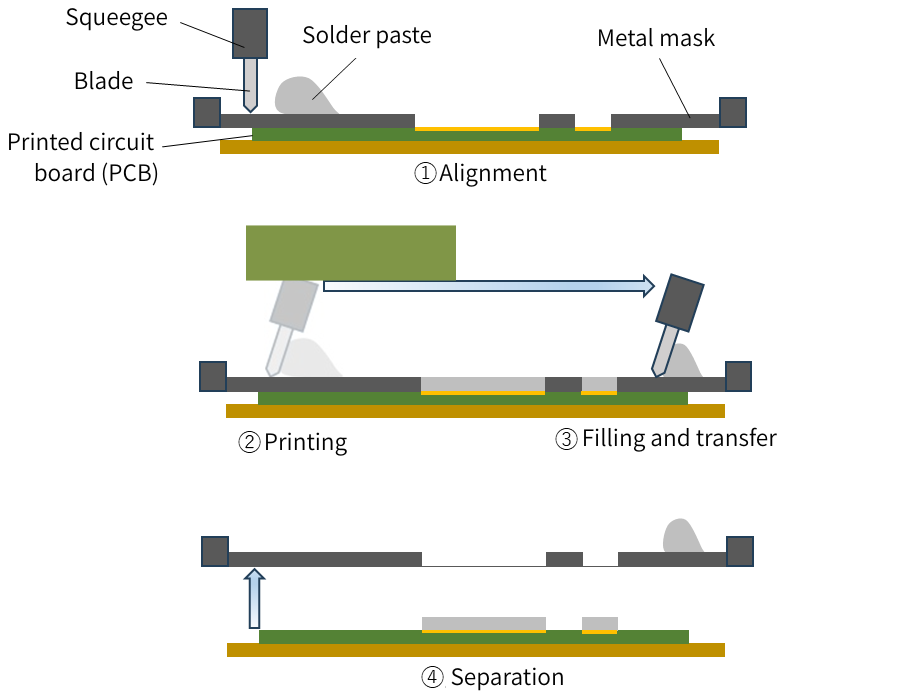
For example, alignment:
Align the printed circuit board and the metal mask so that their openings align precisely.
*The alignment marks on the circuit board and metal mask are recognized by image recognition to perform positional alignment.
② Application:
Solder paste is supplied onto the mask and moved across it with a blade called a squeegee at a constant pressure and speed.
③ Filling and transfer:
As the squeegee moves, the solder paste rolls, increasing the internal pressure and filling the opening in the mask with paste.
④ Separation (Snap-off):
Finally, when the mask is removed from the substrate, the solder paste that filled the openings is transferred to the pads on the substrate, completing the printing process.
② Solder paste inspection
Solder Paste Inspection (SPI)
After solder paste printing, the circuit board is measured using an SPI device that employs cameras, lasers, etc., to numerically measure the "area," "volume," and "position" of the solder, and the quality of the solder printing is inspected by determining whether it passes or fails.
*Some models support automatic feedback control of manufacturing conditions, etc., to the solder printing machine.
○Equipment used
SPI (Solder Paste Inspection) device
○Materials used
Pre-printed circuit board with solder paste
○Steps:
For example, alignment:
The system uses a camera to read the reference marks (Fiducial) on the circuit board and automatically corrects the board's position.
*X coordinate, Y coordinate, Θ
② Imaging and measurement:
Using high-resolution cameras and lasers, measurements are taken and the "area," "volume," and "location" are automatically calculated from the results.
③ Judgment process:
The system compares the result to a set threshold and determines whether it passes or fails.
③ Component mounting
Component mounting (Pick-and-place)
This process involves using a nozzle to pick up and transfer components, then mounting them in the designated position on the circuit board.
*For special parts, custom-made nozzles or chucks may be used to grip and transfer them.
○Equipment used
Surface mount machine (Mounter)
We select and combine equipment according to the components (delivery format, size, shape, required mounting accuracy, etc.).
○Materials used
Pre-printed solder paste circuit boards, various electronic components
○Steps:
For example, alignment:
The system uses a camera to read the reference marks (Fiducial) on the circuit board and automatically corrects the board's position.
② Component adsorption:
The nozzle picks up the parts supplied from the parts supply device.
③ Correction:
A dedicated camera for part recognition measures, inspects, and corrects the position of the part.
*Each item is inspected for its shape, type, polarity, etc., and its coordinates and tilt are corrected.
④ Equipped with:
The program automatically mounts components to the locations specified by the mounting system.
*During installation, we monitor for component suction leakage and control the pressing pressure to maintain the quality of delicate components.
④ Reflow soldering / ⑤ Cooling
Reflow soldering / Cooling
Reflow soldering is a process that involves melting and solidifying solder using heat treatment to connect circuit boards and electronic components.
○Equipment used
Reflow oven
A device equipped with a conveyor belt and a heating furnace divided into multiple zones, capable of uniformly heating substrates.
*For quality improvement, nitrogen (N₂) compatible types are now the mainstream.
○Materials used
Circuit board with components already mounted
○Steps:
Reflow is managed by a heat treatment flow called a "temperature profile".
① Increase in temperature:
The entire circuit board is heated slowly. The temperature rise rate is generally 3°C/second max, uniformly heating the board and components while preparing for flux activation.
It also helps prevent component damage and cracking caused by rapid temperature changes.
② Preheating:
It maintains a constant temperature, minimizing temperature differences between the circuit board, components, and solder paste.
The flux is activated to prepare the solder for melting.
This ensures that the temperature of the entire circuit board is uniform, preventing uneven heating.
③ Main heating:
The temperature is raised to the melting point of the solder, and then soldering is performed.
The molten solder wets and spreads to the pads on the circuit board and the component TERMINALS, forming a connection.
During this process, surface tension helps to align the objects. (Self-alignment)
④ Cooling: The molten solder is cooled and solidified.
The cooling rate is generally a maximum of 6°C/second; if it is too slow, the crystals will coarseen, leading to a decrease in connection strength.
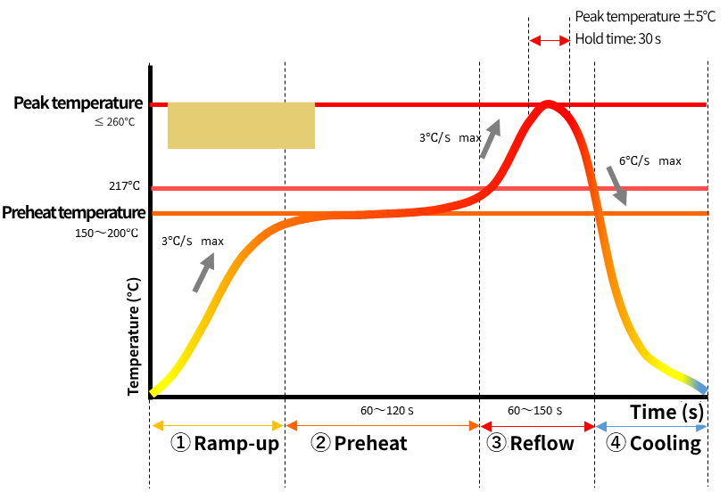
The above is a typical profile for general lead flow soldering.
Please optimize the design to match the characteristics of the materials (solder, components, circuit board, etc.) used on the actual circuit board.
⑥ Visual inspection
Automated Optical Inspection (AOI)
Using a high-resolution camera and lighting, the substrate surface is imaged, and the appearance of the substrate is automatically inspected using image processing.
○Equipment used
AOI device (2D/3D AOI)
While 2D types are the mainstream, there are also devices capable of 3D measurement, and some models can perform more detailed assessments of part height, fillet shape, lead lift, and other parameters.

○Materials used
Circuit board with components already mounted
○Steps:
For example, alignment:
The system uses a camera to read the reference marks (Fiducial) on the circuit board and automatically corrects the board's position.
② Imaging and measurement:
The system uses an imaging camera to capture images and reads the state and shape of the mounted components from those images.
③ Judgment process
The system compares the result to a set threshold and determines whether it passes or fails.
*While this is often done after reflow soldering, it is sometimes performed before reflow soldering as a block guarantee.
X-ray Inspection
Areas where electrodes and connections are not visible from the surface are inspected using internal transmission imaging with X-rays.
○Equipment used
X-ray inspection equipment (2D/3D X-ray)
While 2D types are the mainstream, there are also devices capable of 3D measurement, and some models allow for more detailed assessment by visualizing the interior in three dimensions (CT).
○Materials used
Reflowed PCB
○Steps:
① Circuit board set:
The substrate is placed on the stage of the X-ray apparatus.
② Imaging and measurement:
X-rays are generated, and an image of the substrate through which they pass is acquired.
③ Judgment:
The pass/fail determination is made either by visual inspection or by comparing the image to a threshold set during image processing.
Challenges in the surface mount process
We have explained the flow of each process so far, but now let me briefly introduce the challenges of each.
1. Solder paste printing
Importance
The quality of the printing significantly affects the quality of the soldering.
Incorrect printing conditions (area, volume, and position) can lead to various defects.
Main challenges
Improved solder printing reproducibility (reducing variations such as insufficient, excessive, smudged, and misaligned solder).
Improved stability through metal mask design (thickness, aperture shape, aspect ratio).
Solder paste management (temperature, viscosity, changes over time, etc.)
Addressing the challenges
Optimization of printing conditions: Optimization of squeegee pressure and speed, stencil release speed, support pin position, etc.
Material management: Paste storage management, standardization of room temperature return and stirring, expiration date management.
Mask optimization: Optimization of thickness, improvement of opening shape such as home plate/reverse taper, addition of chemical treatment, etc.
Cleaning metal masks: Optimizing cleaning cycles and rules
②Solder Paste Inspection (SPI)
Importance
Print results are managed numerically (area, volume, position) and corrected to prevent defects from reaching subsequent processes.
Main challenges
Setting thresholds (reduced production volume due to overly strict thresholds / reduced yield in subsequent processes due to overly lenient thresholds)
Thorough implementation of feedback to the printing press
Addressing the challenges
Setting appropriate thresholds through data analysis (it is also advisable to check for correlation with defects after reflow).
Standardize feedback rules for abnormal situations (e.g., plate cleaning, squeegee replacement, print condition changes).
The introduction of automatic/semi-automatic feedback enables immediate adjustment of position, squeegee pressure, speed, and cleaning cycle.
3. Pick-and-place
Importance
The ability to mount components in the correct orientation and position is crucial for quality.
*To ensure that the self-alignment force during reflow is properly utilized.
Main challenges
Missed pickup/poor suction (nozzle wear/dirt, feeder feeding)
Position/rotation accuracy (unstable circuit board correction and component recognition) / component damage
Incorrect or reversed implementation of different product types
Addressing the challenges
Standardized maintenance management: nozzle cleaning/replacement cycle, feeder maintenance, vision calibration (periodic)
Program standardization: XYθ correction, appropriate setting of suction height and pressure conditions.
Utilization of verification systems such as barcode authentication for supplied parts, and utilization of image recognition functions.
④ Reflow soldering / ⑤ Cooling
Importance
The circuit board and components are connected by heating according to the temperature profile and melting the solder.
This is the final joining process that determines the quality of the assembly.
Main challenges
Profile optimization (heating, preheating, main heating, cooling)
Parts damaged due to insufficient heat resistance
Atmosphere control (N₂ concentration, furnace cleanliness)
Soldering defect countermeasures (voids, poor wetting, bridges, tombstones, etc.)
Addressing the challenges
Profile verification and configuration based on actual measurements
Confirmation of compliance with component heat resistance specifications (actual measurement and margin confirmation)
Standardization of N₂ management (concentration standardization, furnace cleaning, etc.)
Metal mask design / Defect prevention through feedback to the printing press
⑥ Visual inspection (AOI: Automated Optical Inspection) / X-ray inspection
Importance
We inspect the visual quality of every single unit after reflow (missing parts, polarity, position, fillets, etc.) to prevent defective products from being shipped.
X-ray inspection can detect defects in the underside joints, such as BGA/QFN, which are not visible externally and cannot be seen with AOI.
Main challenges
Setting thresholds (reduced production volume due to overly strict thresholds / reduced yield in subsequent processes due to overly lenient thresholds)
Feedback to the previous process when defective products occur
Addressing the challenges
Improving imaging conditions (adjusting camera settings and, in some cases, using 3D cameras or laser functions)
Reviewing detection conditions (improving misclassification by reviewing recognition parameters and LOGIC)
We will establish a system for analyzing defective products and implement improvements and countermeasures through early feedback to the upstream process.
NEXTY Electronics Initiatives
NEXTY Electronics Corporation works with ODM/EMS partners with a wealth of experience, primarily engineers with extensive experience in elemental manufacturing technologies, to build schemes to support the launch of a wide variety of industries and products.
We utilize the experience and know-how we have cultivated in a wide range of fields, including automobiles and industrial equipment, to meet the needs of our customers and society and provide new value in manufacturing.
I want to manufacture a circuit board like this!
I'm having trouble with the implementation of ○○!
I need help with parts procurement and PCB assembly
or handle the prototyping with mass production in mind!
If you have any requests or suggestions like this, please feel free to contact us.
Please Inquiry through our website.
https://www.nexty-ele.com/business/design-dev/