
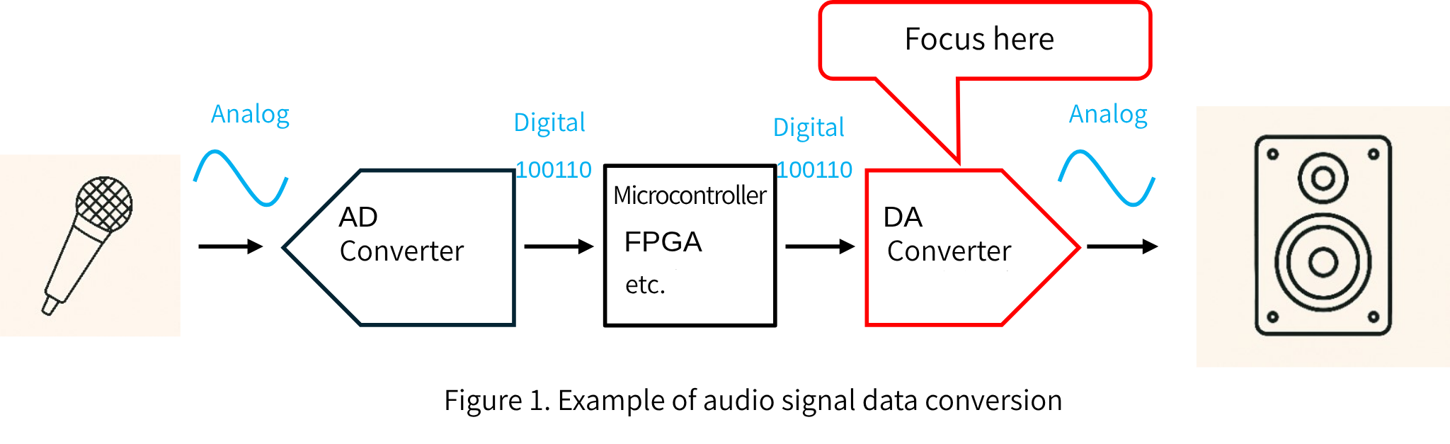
Introduction
In electrical circuit design, the information that humans sense, such as sound and light, is "analog," but control devices such as microcomputers can only handle "digital" information.
Understanding the technology that bridges this gap will enable higher quality product designs.
The following two converters act as a bridge between "analog" and "digital."
- AD converter: converts analog information into digital information
- DA converter: converts digital information into analog information
This time, we will focus on DA converters and explain their main specifications.
Main SPECs
Types of SPEC
SPEC (specification items) can be broadly divided into two types. Representative items for each are listed below.
Static Error
It is mainly related to DC characteristics (direct current characteristics) and indicates the deviation from the ideal output value.
- Resolution: How precisely can analog values be expressed?
- Offset Error: The deviation that prevents ideal zero input from resulting in zero output.
- Gain Error: The deviation of the overall scale (slope) from the ideal value
- Integral nonlinearity (INL): The difference between the code value and the output value within a certain range
- Differential Nonlinearity (DNL): The deviation of output voltage steps between adjacent codes
Dynamic Error
This is mainly related to AC characteristics (ability to follow signals that change over time).
- Settling Time: The time it takes for the output to converge to a certain error range after switching to a new value.
- Glitches: Temporary noises or spikes that occur when digital codes are switched.
- Harmonic Distortion: The introduction of unwanted harmonics into a signal.
- Noise: Random electrical noise
We will explain each item in detail.
Static Error Detailed Explanation
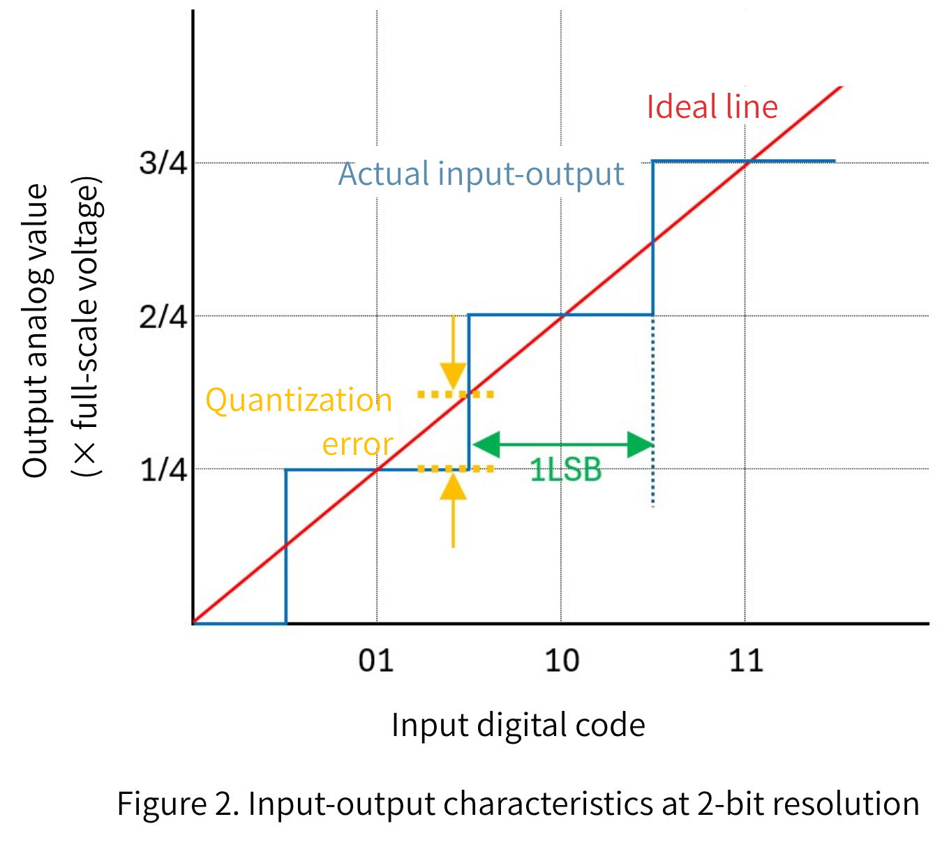
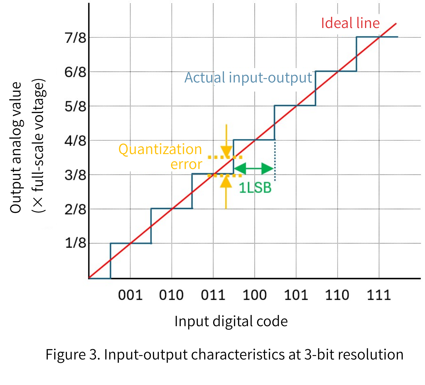
Resolution
The degree to which an analog value can be expressed is determined by an indicator called "resolution." The higher the resolution, the greater the ability to finely adjust the output.
The figure below shows the input/output characteristics for 2-bit and 3-bit resolution. Ideally, the input and output would be proportional in a straight line, as shown by the red line, but in reality, the characteristic becomes stepped, as shown by the blue line, depending on the number of input digital codes that can be expressed by the resolution.
The smallest step in this staircase (green arrow) is called "1 LSB." In principle, an error of 1 LSB/2 will always occur in the output analog value (yellow arrow) relative to the ideal red line. This error is called "quantization error."
The higher the resolution, the smaller the quantization error, but higher resolution also comes with the disadvantages of higher costs and increased data traffic. Therefore, it is important to strike a balance and select the optimal resolution depending on the application.
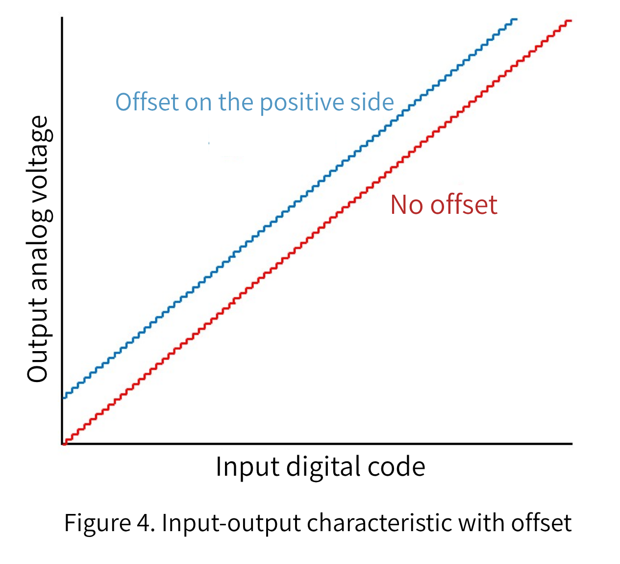
Offset Error
When the input digital code is "0", the output analog voltage should also be 0 V. However, a small voltage (positive or negative) may actually be output. This deviation is called the "offset error."
Because offset error is a constant regardless of the input digital code value, once the amount of error is known, it can be relatively easily corrected by shifting the input digital code in the opposite direction by that amount.
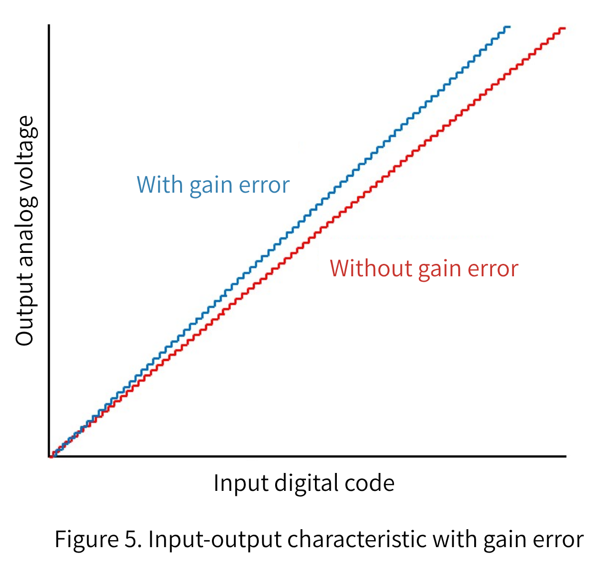
Gain Error
The proportional relationship between input and output remains the same, but if the slope of the output (how it increases or decreases) differs from the ideal, this is called a "gain error."
Unlike offset error, the magnitude of the gain error changes depending on the value of the input digital code. Therefore, when correcting for gain error, it is necessary to measure the actual output value at multiple points and determine the difference in slope from the ideal straight line to perform the correction.
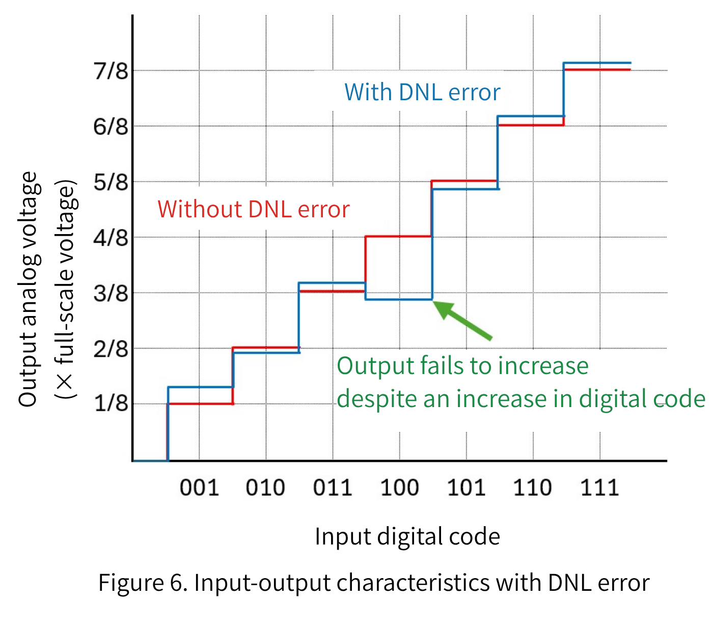
Differential Nonlinearity (DNL)
DNL (differential nonlinearity) is an index that indicates how much the output step width between adjacent digital codes deviates from the ideal 1 LSB (smallest step width). It can be imagined as checking whether all the steps in a staircase are the same height.
Unlike offset error, DNL cannot be easily corrected because it occurs randomly with each digital code.
Normally, the output analog voltage increases by a fixed amount each time the input digital code increases by one. However, if the DNL error is 1 LSB or greater, the output analog voltage may not change or may even decrease when the input digital code is changed by 1 LSB. This is called a "missing code."
When a missing code occurs, the output voltage change in that area becomes unreliable.
At the beginning, we explained that "resolution" determines the performance of the analog output. For example, if the resolution is 14 bits but the DNL error is 3 bits, and if the resolution is 12 bits and the DNL error is less than 1 bit, the latter will actually have higher analog output performance.
As such, DNL is an important SPEC (specification item) just like resolution.
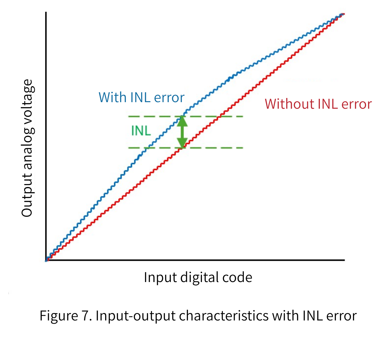
Integral Nonlinearity (INL)
INL (integral nonlinearity) is an index that indicates how far the output analog voltage deviates from an ideal straight line (reference line). It can be imagined as checking whether the entire staircase follows a straight line (see Figure 7).
Unlike gain error, INL cannot be easily corrected because its slope changes with each digital code.
Dynamic Error
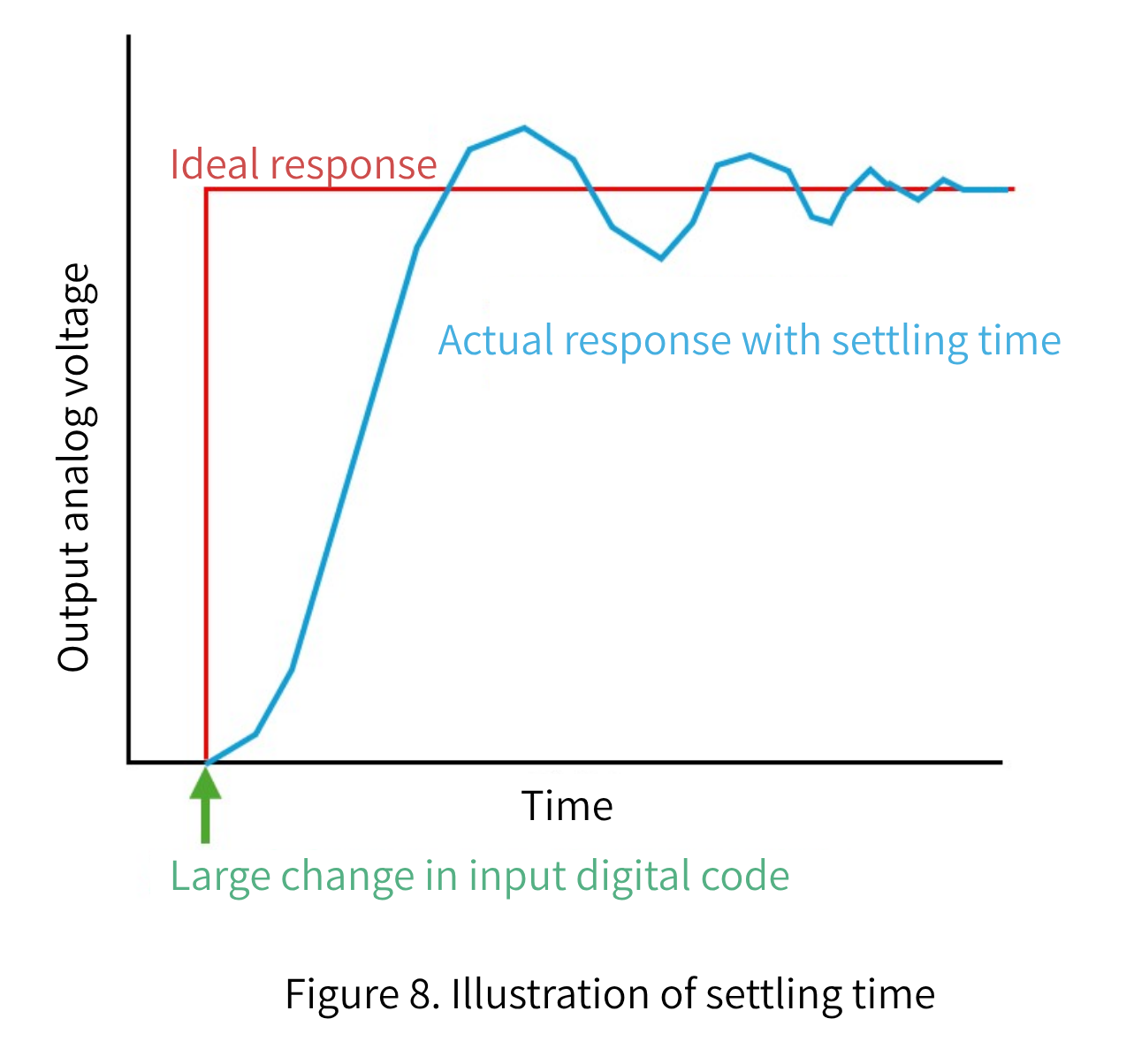
Settling Time
Settling time is the time it takes for the output analog voltage of a DAC to settle to its target value (predetermined voltage) after the DAC output has switched to a new digital code value.
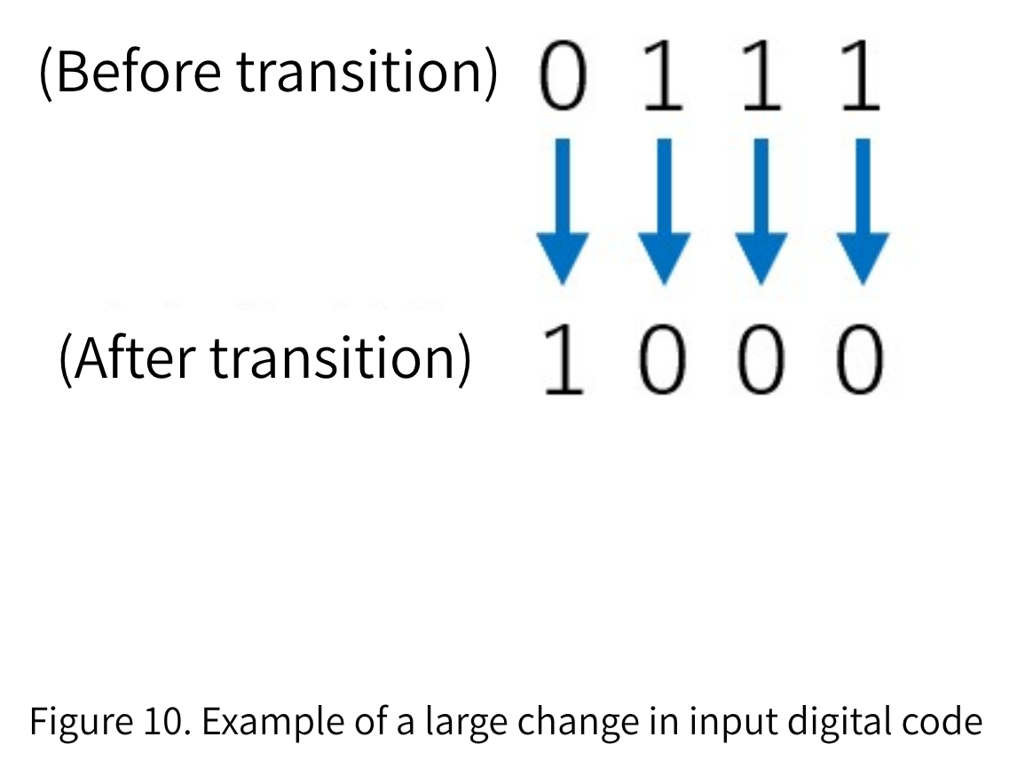
This settling time increases with increasing input digital code change, for example, from the minimum (0000) to the maximum (1111) of a 4-bit code.
If there is ample time in the sampling period (measurement interval), there is no problem if you wait a sufficient amount of time before measuring the stable output voltage. However, if you need to sample at high speed, it is important to choose a highly responsive method such as a "current output DAC" with a short settling time.
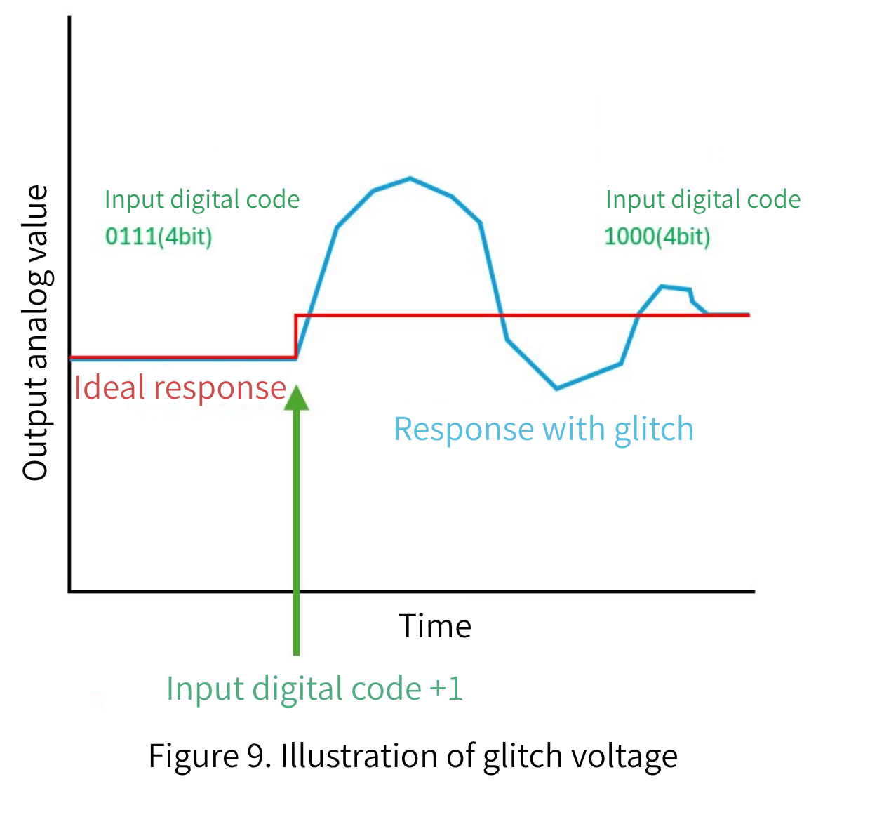
Glitch
A glitch is a short-duration spike-like error voltage that occurs at the moment the DAC's digital code switches.
In particular, when the most significant bit (MSB) of the input digital code switches, all of the binary bits simultaneously change from 0 to 1 or from 1 to 0. At this time, multiple SWITCHES inside the DA converter switch simultaneously, and there is a slight difference in the timing of each SWITCHES switching, causing a glitch.
One way to suppress glitches is to add an analog low-pass FILTERS (LPF) to the output to reduce noise components. There are also products that are designed to prevent all input digital codes from being inverted when the MSB switches inside the DA converter.
Harmonic Distortion
When a sine wave is input into a DA converter, ideally only that frequency should be output, but in reality, extraneous frequency components that are two, three, four times the input frequency, etc., may also be output. These extraneous components are called "harmonic distortion." Harmonic distortion occurs due to nonlinearity within the DA converter circuit, and is closely related to the DNL and INL explained in the static characteristics section.
"THD (Total Harmonic Distortion)" is an index used to express the magnitude of harmonic distortion. THD indicates how many harmonics are contained in relation to the base frequency (fundamental wave). It is an important parameter for audio DA converters, as it has a particular impact on sound quality.
Another similar indicator is SFDR (Spurious Free Dynamic Range). While THD indicates the ratio of the fundamental wave to harmonics, SFDR indicates the ratio of the fundamental wave to the largest unnecessary frequency component other than the fundamental wave. SFDR evaluates not only harmonics but also OTHERS unnecessary signal components, so it is important for DACs used in communications.
Noise Spectral Density (NSD)
"Noise spectral density" is an index that represents the frequency distribution of random noise contained in the analog output of a DA converter. It is generally expressed as voltage spectral density in units of "V/√Hz."
This noise spectrum is formed by a combination of several factors.
- Thermal noise: This is the basic noise that occurs in passive components such as RESISTORS and in the junctions of semiconductors.
- Quantization noise: Noise caused by rounding errors that occur when representing a digital signal using a limited number of bits.
- 1/f noise (flicker noise): Noise that is noticeable at low frequencies, and the lower the frequency, the greater the noise power.
- Clock jitter: This is noise generated by fluctuations in the timing of the sampling clock, and has a particularly large effect on high-frequency output signals.
- POWER SUPPLIES /GND noise: Noise that enters from the outside through POWER SUPPLIES or GND lines.
Finally
Above, we have explained the main specifications of the DA converter.
By correctly understanding each specification item and selecting and designing the optimal product for the application, you can improve the quality of your electrical circuit design and prevent problems.
For more detailed technical information and related products, please use the related columns and Inquiry form below.
Inquiry
Related Product Information
車載向け光センサーで明るさを検出 VEML6031
車載向け光センサーVEML6031は、スポーツカーの車速にも正確に応答し、太陽光から低透過率ガラスを介した光まで、広範囲の明るさを測定することができます。
- Vishay Intertechnology, Inc.
- NEXT Mobility

Low-Power MCU with AI Accelerator for Edge AI
The MAX78000 series enables AI processing on low-power edge devices, enabling real-time processing of applications such as machine vision, audio, and facial recognition.
- Analog Devices, Inc.
- NEXT Mobility
- ICT and Industrial
- Smart Factories and Robotics

OptiMOS™ revolutionizes POWER SUPPLIES design with high-efficiency, high-reliability power MOS FETS. ~ Accelerate next-generation POWER SUPPLIES design with OptiMOS™ ~
Infineon's OptiMOS™ achieves low on-resistance and high-speed SWITCHES, making it a highly reliable power semiconductor for automotive and industrial applications.
- Infineon Technologies AG
- NEXT Mobility
- ICT and Industrial
- Smart Factories and Robotics
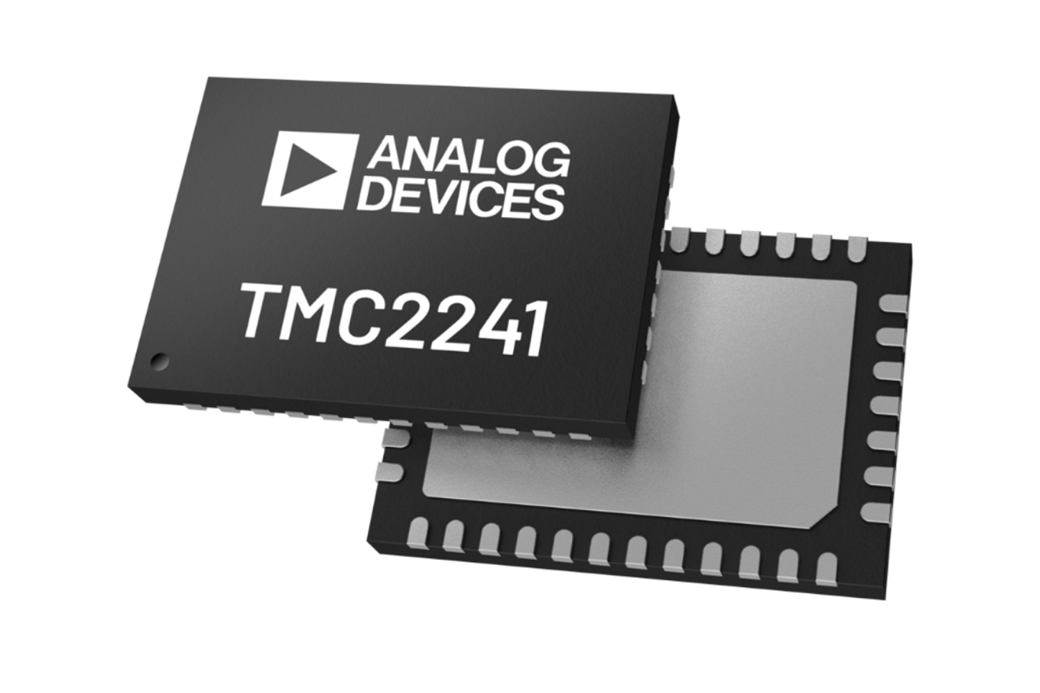
TMC2241: 65V 2-arm smart built-in stepper motor driver (with S/D and SPI)
The TMC2241 is a high-performance ROTATIONAL STEPPING MOTORS driver IC compatible with 65V. It features quiet operation and current sensing capabilities.
- Analog Devices, Inc.
- ICT and Industrial

An In-Depth Look at the Features of NXP's Automotive CAN/LIN Transceiver Products
This article explains the features of NXP’s automotive CAN/LIN transceivers, designed to withstand harsh in-vehicle conditions, for ECU developers looking for reliable in-car network products.
- NXP Semiconductors NV
- NEXT Mobility
- ICT and Industrial

Introducing NXP's CAN TRANSCEIVER products with signal improvement (SIC)
NXP's SIC-equipped CAN TRANSCEIVER actively suppresses ringing on the transmitting side, stabilizing high-speed CANFD communications. It is software and pin compatible, allowing it to be replaced with existing designs, and is compliant with automotive standards.
- NXP Semiconductors NV
- NEXT Mobility