
FETs are essential semiconductor elements for SWITCHES circuits and POWER SUPPLIES design, but improper selection can lead to reduced efficiency and reliability issues. Characteristics such as on-resistance, feedback capacitance, and gate threshold voltage are particularly directly linked to loss and heat generation. This article therefore provides a practical overview of five performance indicators to consider when selecting a FET, as well as robustness and cost considerations to keep in mind during design. It explains the basics of achieving both efficiency and reliability, including conservative estimates for initial design and trade-off considerations.
Five performance indicators to consider when selecting a FET
The following five characteristics mainly affect the performance of a FET:
- Rds(on): On-resistance
- CRSS/CGD: Reverse transfer capacitance/Gate-drain capacitance
- Vgs(th): Gate voltage threshold
- Qg: Gate charge
- Parasitic DIODES
I will explain these in order.
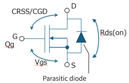
FIGURE 1.FET
Rds(on): On-resistance
This is the resistance between the drain and source TERMINALS when the FET is on. This value tends to be proportional to the FET's die temperature and is also heavily dependent on the Vgs voltage. Therefore, it is important to always check the conditions under which Rds(on) is specified in the datasheet, as shown in [Figure 2. Rds(on) and Conditions]. The conduction loss, which is greatly affected by Rds(on), can be calculated using the following formula.
Conduction loss [W] = on-resistance [Ω] x effective current [A] x on-time [s]/sec
| SPECIFICATIONS (T J = 25 °C, unless otherwise noted) | ||||||
|---|---|---|---|---|---|---|
| PARAMETER | SYMBOL | TEST CONDITIONS | MIN. | TYP. | MAX. | UNIT |
| Static | ||||||
| Drain-source on-state resistance a | R DS(on) | V GS = -10 V, I D = -15 A | - | 0.0079 | 0.0096 | Ω |
| V GS = -4.5 V, I D = -15 A | - | 0.010 | 0.0122 | |||
FIGURE 2. RDS(ON) and Conditions
CRSS/CGD: Reverse transfer capacitance/Gate-drain TERMINALS capacitance
CRSS refers to the capacitance that causes the Miller effect, while CGD refers to the physical capacitance between TERMINALS. Both definitions roughly mean the same capacitance, and the smaller the value, the steeper the rise and fall of the square waves generated by INVERTERS and SWITCHING POWER SUPPLIES, increasing SWITCHES noise. During initial design, we recommend using the following formula to estimate transition loss on the safe side (as shown in the formula, transition loss and CRSS are proportional).
Transition loss [W] = 2 x Maximum voltage [V] 2 x Maximum current [A] x CRSS [F] x SWITCHES frequency [Hz]
If the application is not SWITCHES, there is no need to place importance on CRSS. There is also a trade-off between a small CRSS and the SOA (safe operating area) tolerance, which will be described later.
VGS(th): Gate voltage threshold
A large number of FET cells are lined up inside a FET, and when all of these are turned on, Rds(on) is formed.
There is a difference between cells in the turn-on Vgs(th), and Vgs(th) refers to the minimum voltage at which at least one of the cells turns on. If the device is operated near Vgs(th), current will concentrate in some cells, posing a risk of destruction, so a design with sufficient margin is required.
Qg: Gate charge
This is the amount of charge that must be supplied to the gate TERMINALS to turn the FET on. In SWITCHES circuit, this amount of charge is required each time the FET is turned on, and the average input current to the gate can be calculated using the following formula.
Average input current to the gate [A] = gate charge [C] x SWITCHES frequency [Hz]
Parasitic DIODES
A parasitic DIODES is formed in the FET from the source to the drain. In SWITCHES applications, DIODES is required here to prevent back electromotive force, but the parasitic DIODES has poor characteristics, so an instantaneous voltage drop and loss occur. This can be prevented by attaching an external high-speed DIODES as needed. The important characteristic values of this DIODES are:
Forward voltage VF [V], reverse recovery time trr [s], and rise/fall time ton/off [s].
Design points to improve FET robustness
Robustness refers to the ability of a FET to maintain reliability and not be destroyed during operation. To achieve this, it is essential to design the FET so that its absolute maximum ratings and tolerances are not exceeded. Four particularly important items in this regard will be explained below.
Vds: drain-source voltage rating
If the Vds value is exceeded, the FET will break down and enter the avalanche region. In theory, it will not break down if used below its avalanche energy tolerance, but since this tolerance is small, it is recommended to use it below the rated voltage. In particular, in SWITCHES circuits, unexpected high voltages can occur instantaneously, so it is necessary to check this by appropriate waveform observation.
Pd: Power dissipation
This is the power loss that the FET can consume at any given time. This value varies depending on factors such as the ambient temperature and board conditions, so it is important to calculate the thermal resistance using simulations or other methods, referring to the values listed on the datasheet, and consider whether the FET can withstand the loss. Note that loss Pd is the sum of the transition loss and conduction loss mentioned above.
Tj: Junction temperature rating
This is the maximum allowable temperature of the semiconductor (die) inside the package. Since Tj cannot be measured directly, it is calculated backwards using the case temperature and thermal resistance (RthJC), etc.
SOA: Safe Operating Area
This is an index showing the pulse withstand capability of a FET and is shown in the image on the left in the diagram below. Exceeding any of these limit lines could destroy the FET, so it is necessary to stay below that line. Sufficient margin is particularly necessary near the secondary breakdown limit line. The power limit line on the SOA curve can be adjusted by referring to the derating curve. For example, as shown on the right in the diagram below, if a loss of 200W is possible at 25°C and 100W at 75°C, the current value of each SOA limit line at 75°C will be half that at 25°C (100W/200W).
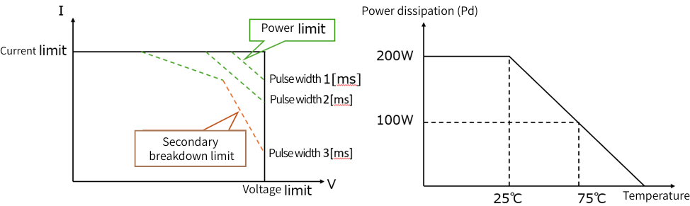
FIGURE 3. SOA curve and derating curve image
Summary
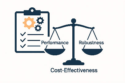
When selecting a FET, capacitance characteristics such as on-resistance and CRSS determine efficiency, while threshold voltage and SOA compliance are essential for ensuring reliability. Since there is a trade-off between performance, robustness, and cost, it is important to design according to the application. We recommend that you make conservative loss estimates using maximum voltage and current in the initial stage, and then adjust these using simulations and measurements in the detailed design. We offer optimal FET selection and technical support, so please visit our product page.
Inquiry
Related Product Information

Key points of GMSL2 design
This article explains the features and design key points of Analog Devices' next-generation GMSL, GMSL2.
- Analog Devices, Inc.
- NEXT Mobility
Introducing the next generation semiconductor, SiC Schottky diode
We will provide a detailed explanation of Vishay's SiC Schottky DIODES, which achieve a breakdown voltage of 1200V and feature high speed and low VF.
- Vishay Intertechnology, Inc.
- ICT and Industrial
- Smart Factories and Robotics

Introduction to Edge AI Solutions with NXP's NPU-equipped i.MX/MCX
This article explains the rapidly growing edge AI with real device examples and introduces NXP’s processors and microcontrollers equipped with NPUs.
- NXP Semiconductors NV
- NEXT Mobility
- ICT and Industrial
- Smart Factories and Robotics

Introduction to NXP's Automotive Millimeter-Wave Radar Products
This article provides an overview of automotive millimeter-wave radar, a key sensor in advanced driver-assistance systems (ADAS), and introduces NXP’s leading radar product family driving the market.
- NXP Semiconductors NV
- NEXT Mobility
- ICT and Industrial
- Smart Factories and Robotics

Solving the Challenges of Battery Voltage Fluctuations in Automotive Applications
In automotive applications, battery voltage can fluctuate during operation. We introduce the MAX20039/MAX20040 as a solution to this problem.
- Analog Devices, Inc.
- NEXT Mobility

CoolSiC™ MOS FETS "CoolSiC™ MOS FETS supports next-generation electrification" High efficiency, high voltage resistance, and high reliability. SiC power MOS FETS ideal for EVs, renewable energy, and industrial equipment.
Infineon's CoolSiC™ MOS FETS offer high voltage resistance, low loss, and high temperature operation, contributing to improved efficiency and reliability of EV and industrial POWER SUPPLIES.
- Infineon Technologies AG
- NEXT Mobility
- ICT and Industrial