As the name suggests, a VD (voltage detector) is a product that monitors voltage.
They are also called voltage detectors, voltage monitoring ICs, reset ICs, etc.
Last time, we introduced the main uses of VDs (voltage detectors), their circuit elements, and the features of each type.
This time, we will introduce applications using external VD (voltage detector) components.
Application of the reset IC with external components
①High voltage POWER SUPPLIES monitoring
I want to use a reset IC to monitor a high-voltage POWER SUPPLIES, but the input voltage rating of the IC will be exceeded.
⇒This can be achieved by using external resistors R1 and R2.
*Note ①:
The input voltage will drop by the IC's current consumption x R1, so it is not good to make the resistance value too large (e.g., 100kΩ or less).
In addition, the through current at the time of detection and release
VIN dropped ⇒ detected again
Detection ⇒ Release through current...
This may cause " hiccups."
The hiccup phenomenon can be prevented by inserting Cin between the resistor and the VIN TERMINALS.
*Note ②: Leak current occurs due to external resistors (VIN/(R1+R2)).
*Note ③: The relative accuracy of resistors R1 and R2 will cause large variations.

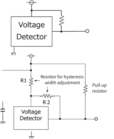
②Increase the hysteresis width
I want to set the hysteresis width larger.
⇒This can be achieved by using external resistors R1 and R2.
As the release voltage increases, the hysteresis width also increases (the detection voltage does not change).
Detection voltage = Vdet
Release voltage = Vdet + Vhys
Hysteresis width = Vhys
Detection voltage = Vdet
Release voltage = (1+R1/R2) × (Vdet + Vhys)
Hysteresis width = (R1/R2) × Vdet + (1+R1/R2) × Vhys
*The hysteresis width cannot be reduced by using an external circuit.
*As with Application ➀, it is not good to make the resistance value of R1 too large.
③ Higher accuracy of release delay time
To shorten the time from POWER SUPPLIES on to device startup completion, the release delay time needs to be made more accurate than the IC's specified value.
⇒ Improved accuracy of release delay time with external resistor RD2 *This may not be applicable depending on the product.
・ The built-in resistor RD varies by about ±50%
RD2<<RD, RD is not used and CAPACITORS is charged with RD2.
・ External resistors are available with high accuracy of ±2% or less, including temperature characteristics.

By reducing the variation in R, the variation in release delay time is reduced.
VTCD;CD TERMINALS threshold voltage

Inquiry
Link to Related Technical Columns
Related Product Information

Low-Power MCU with AI Accelerator for Edge AI
The MAX78000 series enables AI processing on low-power edge devices, enabling real-time processing of applications such as machine vision, audio, and facial recognition.
- Analog Devices, Inc.
- NEXT Mobility
- ICT and Industrial
- Smart Factories and Robotics
LT7176:デジタル・パワー・システム・マネージメント機能を備えた24A/4V、単相または2相Silent Switcher 降圧レギュレータ
LT7176は、最大24A出力に対応するSilent Switcher採用の降圧レギュレータで、PMBus制御やテレメトリ機能、PolyPhase動作も備えています。
- Analog Devices, Inc.
- ICT and Industrial
MAX17639: 3V to 36V, 6A/8A/10A, 12A peak, high-efficiency synchronous step-down DC/DC converter
The MAX1763x is a high-efficiency step-down DC/DC with 3V to 36V input and up to 10A (12A peak) output, featuring integrated MOS FETS, a temperature monitor, and external clock synchronization.
- Analog Devices, Inc.
- ICT and Industrial
- Smart Factories and Robotics
AD4080: 20-bit, 40 MSPS, differential SAR ADC
The AD4080 is a 20-bit, 40 MSPS high-speed, low-noise SAR ADC that provides high-precision data acquisition with wide bandwidth. Evaluation boards and simulation models are available.
- Analog Devices, Inc.
- ICT and Industrial
- Smart Factories and Robotics
MAX77726/MAX77727: 22V, 3A synchronous step-down converter (with ultrasonic mode)
The MAX77726/MAX77727 are high-efficiency step-down converters for ultra-low power devices. They support ultrasonic mode and I2C control.
- Analog Devices, Inc.
- ICT and Industrial

Reduced power consumption through edge processing 3rd generation MEMS sensor
Introducing the iNEMO™ inertial module, a monolithic integrated accelerometer and gyroscope sensor. It allows for some data processing within the sensor, and makes it easy to implement other functions.
- STMicroelectronics
- NEXT Mobility
- ICT and Industrial
- Smart Factories and Robotics
