In many design environments that have experienced fluctuations in semiconductor supply in recent years, product design that takes supply risks into account is becoming common practice. To increase the possibility of component substitution, it is important to consider package compatibility from the early stages of design. By selecting footprints and pinouts that comply with JEDEC standards, switching to products from other manufacturers becomes easy even in the event of a sudden inventory shortage, minimizing the burden of re-layout and jig changes. This column will clarify the relationship between generic names (JEDEC standard names) and STMicroelectronics (hereinafter referred to as ST), and provide a detailed explanation of the advantages and uses of representative packages, as well as how to select them from a BCP perspective.
Why is BCP a design requirement?
Learning from the recent unstable semiconductor supply, there is a rapidly growing trend to emphasize BCP (Business Continuity Planning) when selecting products. In particular, there are an increasing number of cases where products with incompatible packages are not adopted due to the difficulty of substitution. If compatibility is ensured, it is possible to minimize the scope of re-verification of existing PCB land patterns, mounting jigs, mounting profiles, and thermal designs. Conversely, designs that rely on dedicated packages have limited freedom in selecting alternatives, resulting in significant rework due to re-layout and reliability re-testing.
ST promotes package design that complies with JEDEC standards and ensures compatibility with other companies' products, thereby increasing user design freedom and ensuring a stable supply. Particularly in the field of power semiconductors, standardizing physical footprints and pin layouts reduces the risks of design changes and component procurement. Here, we will summarize the requirements that component users place importance on from a BCP perspective.
Required BCP
In BCPs (Business Continuity Plans), the "ability to replace parts immediately" in the event of supply disruptions or delivery delays is crucial, so semiconductor package compatibility (physical, electrical, and process compatibility) is particularly important. With the exception of some products with specialized functions, relying on a single source or dedicated package concentrates supply chain risk, so there is a general trend toward standardizing design and purchasing on the premise of interchangeable packages. In addition to packaging, there are a wide variety of items that require compatibility, but the most common items and their contents are explained below.
1. Footprint/pin compatibility
Standard footprint and pin layout that can be swapped into existing PCBs (replacement with the same land pattern is possible).
2. Electrical Compatibility
The electrical characteristics (voltage range, pin functions) of POWER SUPPLIES, ground, and input/output must remain within the allowable range after replacement.
3. Thermal and mechanical compatibility
Heat dissipation performance, reflow profile, board stress and height (CONNECTORS interference) must be within the allowable range.
4. Mounting and inspection compatibility
It can be handled using existing mounting equipment (mounters, reflow ovens, inspection equipment, jigs) without additional investment.
5. Test and Reliability Data
Reliability test results (HTOL, temperature cycle, humidity, etc.) and qualification data for alternative packages shall be provided.
6. Documents/Libraries
Product datasheets, 3D models, pattern libraries for LGA/QFN, etc., and design guidelines must be prepared.
7. Securing multiple sources of supply
The same specifications can be supplied by multiple vendors, or a cross-reference (interchangeable parts list) exists.
8. Lifecycle Warranty
Commitment to long-term supply, advance notice (EOL/obsolescence) and replacement.
9. Compatibility of handling conditions
MSL (Moisture Sensitivity Level) and storage/transport conditions are acceptable for the current line.
10. Regulatory Compliance
Compliant with RoHS, REACH, and other regulations, as well as customer-specific standards.
List of major packages for ST power semiconductors
This article explains the compatibility between the proprietary names used by some STMicroelectronics power semiconductors (Si-MOS FETS, SiC FET, GaN, Diode) and the JEDEC standard names.
This list compares JEDEC standard names with ST's proprietary names for power semiconductors, and is organized to enable quick design selection. In particular, package compatibility can be confirmed at a glance, making it useful as a guide for selecting packages for ST products from a BCP perspective.
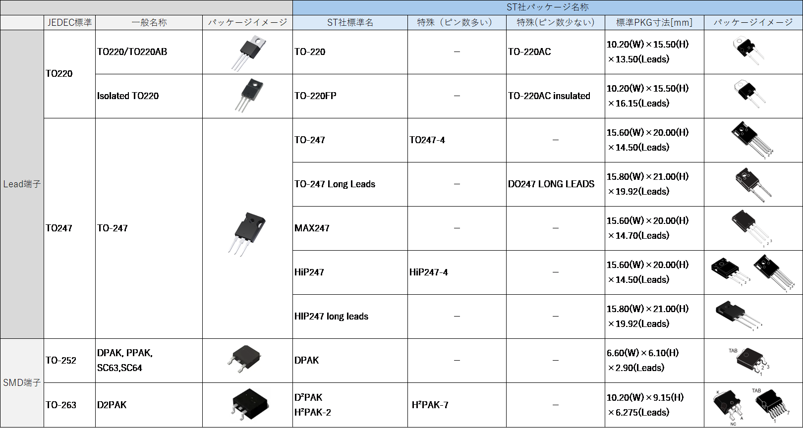
Correlation between JEDEC standards and ST's package names
We will explain the specifications and main features of each package in order.
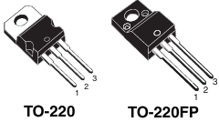
TO-220 package
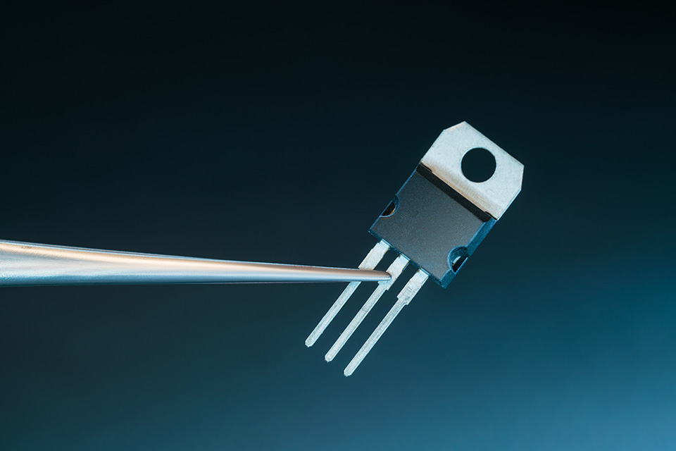
This is the most familiar general-purpose package suitable for medium-power SWITCHES and linear control. It can be directly connected to a heat sink with screws, making it easy to predict heat even at the prototype stage and providing high reproducibility in thermal design during mass production. The JEDEC name is TO-220, and ST's name is the same.
Usage example
Because there is a high degree of freedom in selecting heat sinks and the configuration makes it easy to dissipate heat outside the housing, this type is used in medium-power SWITCHES for automotive ECUs, linear regulators for industrial equipment, simple low-side SWITCHES, and more.
- Standard pin count: 3 pins
- Excellent heat dissipation, allowing for heat sink attachment
- Mounting method: Through-hole
- ST company product name: TO-220
- JEDEC standard: TO-220
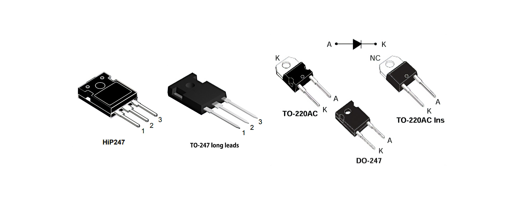
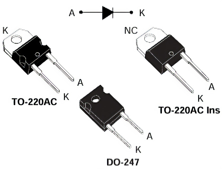
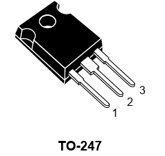
TO-247 package
This is a large package that is frequently used in high-power SWITCHES applications (vehicle INVERTERS, industrial motors, DC link peripherals).
It is compatible with large heat sinks and is easy to ensure a safety distance (creep distance) when combined with an insulating sheet or insulating bushing. In addition to the standard TO 247, ST also offers variations such as the HiP247 (derived type) and TO 247 long leads. The 4-pin version provides an independent Kelvin source, making it suitable for designs that improve SWITCHES loss and gate drive stability.
Usage example
Because of its strength in easily achieving both heat dissipation and high-voltage safety, it is used in high-voltage SWITCHES using SiC FETs, the arms of three-phase INVERTERS, and PFC SWITCHES elements.
- Standard pin count: 3 or 4 pins
- Large heat sink compatible
- Mounting method: Through-hole
- ST company product name: TO-247
- JEDEC standard: TO-247
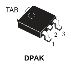
TO-252 (DPAK) package
This compact, low-profile surface-mount package is suitable for high-density mounting. It is suitable for designs that require heat dissipation on the copper surface of the board, such as low-side SWITCHES and DC/DC synchronous rectification. The JEDEC name is TO-252, and ST's name is DPAK. This is advantageous when you want to avoid through-holes and in enclosures with strict height restrictions.
Usage example
They are used in battery management SWITCHES, in-vehicle body control drivers, and secondary-side rectification in industrial POWER SUPPLIES. They are easy to standardize on mounting lines, which is advantageous when starting up mass production.
- Standard pin count: 3 pins
- Compact and low-profile design for easy mounting on a circuit board
- Mounting method: SMD (surface mount)
- Company T product name: DPAK
- JEDEC standard: TO-252
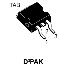
TO-263 (D2PAK) package
Because it has a larger heat spreader surface than DPAK, it is advantageous for SWITCHES that requires high current and high heat dissipation. By combining a larger copper surface with thermal vias, it is possible to design the board so that it can generate heat without a heat sink. The JEDEC name is TO-263, and ST calls it D2PAK. Even for products with strict enclosure height restrictions, there is flexibility in the board design to handle heat dissipation.
Usage example
The mounting equipment is highly versatile and easy to select as an alternative. They are used in high current rectification in communication base stations and industrial POWER SUPPLIES, as well as in automotive power SWITCHES elements.
- Standard pin count: 3 pins
- Ideal for high current and high heat dissipation applications
- Mounting method: SMD
- ST company product name: D2PAK
- JEDEC standard: TO-263
Points to note when selecting a package
When selecting a package, you should pay attention to the following points:
- Compatible with existing board land patterns
- Compatibility with mounting equipment (reflow ovens, mounting machines)
- Heat dissipation design (presence or absence of heat sink, board area)
- Matching pin arrangement and electrical characteristics
- Availability of reliability test data
When considering substitution across mounting methods, physical compatibility alone is not enough. For example, when switching from TO-247 to D2PAK, the heat flow path (direct heat sink vs. PCB spreader) and creep distance are different, so voltage and thermal design must be reevaluated. Mounting and mechanical requirements, such as reflow conditions, MSL, board stress, and height interference, must also be reconfirmed.
In addition, from a BCP perspective, it is important to check whether the pin function assignments (POWER SUPPLIES, ground, input/output) and voltage range/ SWITCHES characteristics are within the acceptable range, and whether reliability test data is available.
You can design more safely by utilizing application notes and design guidelines related to implementation from each company and incorporating them into your design checklist.
Summary
ST's power semiconductors come in a wide range of packages that comply with JEDEC standards, allowing you to select products with BCP measures in mind from the design stage. Checking package compatibility helps reduce supply chain risks and improve design efficiency. If you would like detailed product selection or sample arrangements, please feel free to contact our ST product representatives.
Related Info
ST related product page