The loss, EMI, heat, and cost of SILICONE MOS FETS vary depending on the structure (Planar/Trench/SJ). Therefore, it is important to select an appropriate device according to the voltage range and circuit operating conditions to be used.
Planar (horizontal) transistors are easy to manufacture and suitable for general-purpose low- to medium-voltage applications, but they have low cell density and slightly larger on-resistance Rds(on). Trench (vertical) transistors use a vertical gate structure to increase cell density, achieving low on-resistance Rds(on) and excellent SWITCHES characteristics, and are widely used in low- to medium-voltage, high-efficiency applications. Superjunction transistors achieve low conduction losses even in the high-voltage range by compensating for charge with P/N SILICONE pillars, making them advantageous for increasing the withstand voltage of POWER SUPPLIES and converters.
STMicroelectronics (hereinafter referred to as ST) has these technologies in place and offers a range of MOS FETS optimized for industrial, automotive and consumer electronics applications, from low-voltage trench to medium-voltage planar and high-voltage superjunction, with minimum supply-life commitments for these products.
This article provides diagrams and practical know-how on selection criteria for different applications, differences in mechanisms, and an introduction to ST's MOS FETS product lineup, making it useful for making decisions when adopting MOS FETS products.
MOS FETS structure and features
The device structures of power MOS FETS, such as "Planar," "Trench," and "Super Junction," differ in the design of the electric field distribution in SILICONE, channel width, and drift region, which results in different trade-offs in performance such as on-resistance Rds(on), breakdown voltage, SWITCHES characteristics, thermal characteristics, and manufacturing cost. Below we will explain the characteristics of each structure and how they result in different characteristics.
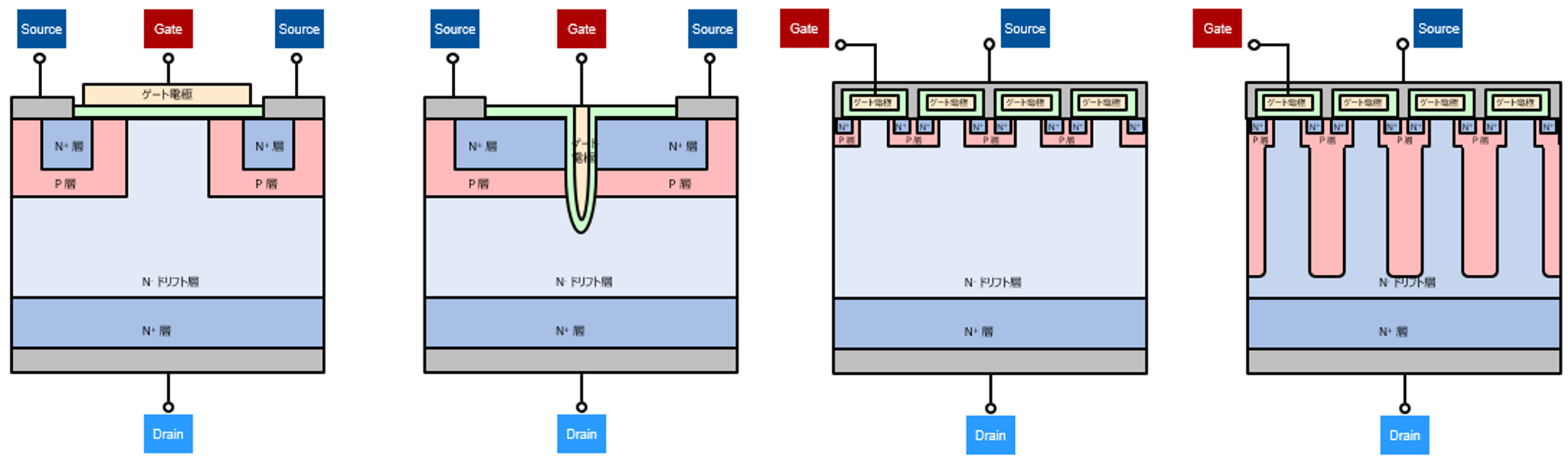
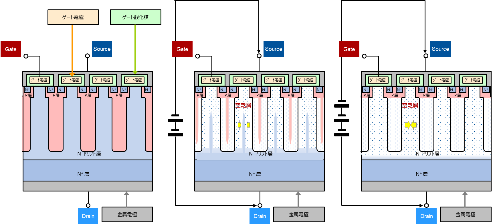
Typical MOS FETS structure diagrams (planar/trench, high-voltage planar/superjunction)
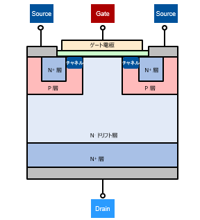
Planar type
This is a conventional structure, with the gate and channel formed on the surface of the chip, and the channel for electrons formed laterally. Manufacturing is relatively simple, and the electric field distribution is straightforward, so avalanche resistance and durability tend to be good, but there are limits to cell density and channel width for the same voltage class, resulting in a higher on-resistance per unit area (Rds(on)). This type MOS FETS is often used in low to medium voltage (e.g., up to 250V) and in applications where shock resistance is important.
Planar type basic structure
Trench type
By forming the channel, which is the path for electrons, on the side of a deep trench, the channel width per unit area can be expanded, significantly reducing the on-resistance Rds(on). This results in excellent low resistance and high efficiency, and is widely used in high-performance SWITCHES in the low to medium voltage class. However, the trench structure changes the behavior of the gate-drain (Miller) capacitance and gate charge, which can affect the Miller effect and SWITCHES losses during SWITCHES. Furthermore, compared to planar types, the manufacturing process is more complex due to the additional step of etching the gate electrode down to the drift layer.
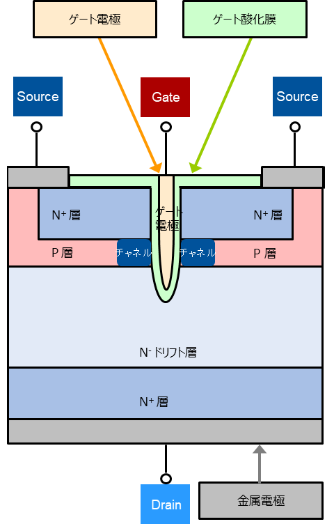
Trench type basic structure
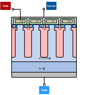
Super Junction (SJ) type
To overcome the trade-off between high breakdown voltage and low on-resistance Rds(on) (increasing breakdown voltage usually results in higher on-resistance Rds(on) = also known as SILICONE limit), the drift region is alternately divided into p-type and n-type pillars (charge balance in the drift region, not the channel) to homogenize the electric field distribution. As a result, extremely low on-resistance Rds(on) can be achieved in the high-voltage range of 400V to 1700V. However, high-precision charge balance is required in manufacturing, which increases the difficulty in terms of cost and yield. SWITCHES characteristics and recovery characteristics also behave differently from conventional types, so these characteristics must be taken into consideration when designing the circuit.
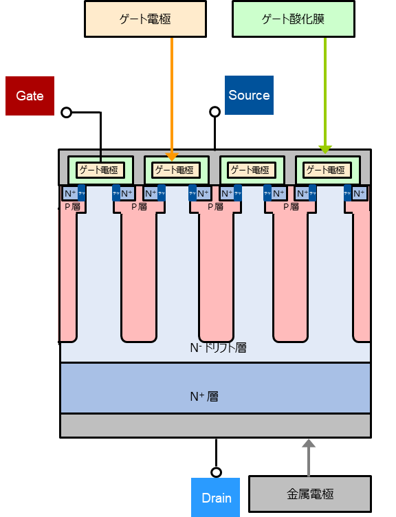
Superjunction (SJ) type basic structure
Summary of features of planar/trench/superjunction MOS FETS
The following is a functional overview of the features of the planar/trench/superjunction types.
| type | Planar | trench | Super Junction |
|---|---|---|---|
| Schematic diagram |
|
|
|
| structure | Horizontal type (channel: horizontal) | Vertical type (channel: vertical) | Superjunction type |
| pressure resistance | 〇 to several hundred volts | △ ~ 100V | ◎ Several hundred to 1700 or 2000V |
| density | × High density is difficult | ◎ High density possible | ◎ High density possible |
| On-resistance | △ Tends to be relatively expensive (large per unit area) | Significantly smaller than the planar type (Especially advantageous at low voltages) | ◎ Very small (Very small even at high voltages) |
| SWITCHES speed | Drive side: △ Medium Recovery characteristics: × Gradual | Drive side: × Large Qgd and gate charge Recovery characteristics: △ Slow | Drive side: × Large Coss and parasitic capacitance Recovery characteristics: △ Soft recovery is difficult to achieve |
| Manufacturing costs | ◎ Good yield | Moderate (good mass production effect) | × The process is the most difficult (poor yield) |
| advantage | Excellent avalanche resistance and shock resistance, and cost-effective. Suitable for applications where low frequency and durability are important. | Low on-resistance per unit area: Excellent Rds(on) and high efficiency for low to medium voltages. General-purpose high performance. | The on-resistance (Rds(on)) in the high voltage region is extremely small. Suitable for high voltage applications such as SWITCHING POWER SUPPLIES and power conversion. |
| Disadvantages | At the same breakdown voltage, the on-resistance (Rds(on)) is high, which is disadvantageous for low-voltage SWITCHES that prioritize efficiency. | In high-speed SWITCHES circuits, care must be taken in gate drive/snubber design. | High cost and low yield. Parasitic capacitance and recovery behavior are design challenges. |
Feature summary comparison table
Deep dive into the features of each MOS FETS structure
From here, we will use structural diagrams to look at the differences in operation between planar, trench, and superjunction.
Differences between planar and trench types
The planar type is also known as a horizontal structure, as the gate is attached to the surface of the wafer, while the trench type is known as a vertical structure, as the gate is embedded in a vertical groove dug into the wafer.
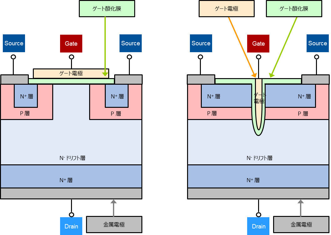
Comparison of basic structures between planar and trench types 1
When a voltage (gate voltage) is applied between each source and gate TERMINALS, a channel is formed, which is a path for electrons, allowing current to flow. This channel is formed horizontally in the planar type, while it is formed vertically in the trench type. The direction in which this channel is formed is the biggest difference between the two.
Comparison of basic structures between planar and trench types 2
When a voltage is applied between the source and drain TERMINALS with the channel formed, electrons can pass between the drain and source TERMINALS, allowing current to flow through the FET.
Comparison of basic structures between planar and trench types 3
Now let's dig a little deeper into how it works.
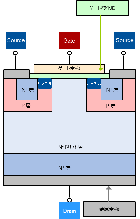
Planar type
-
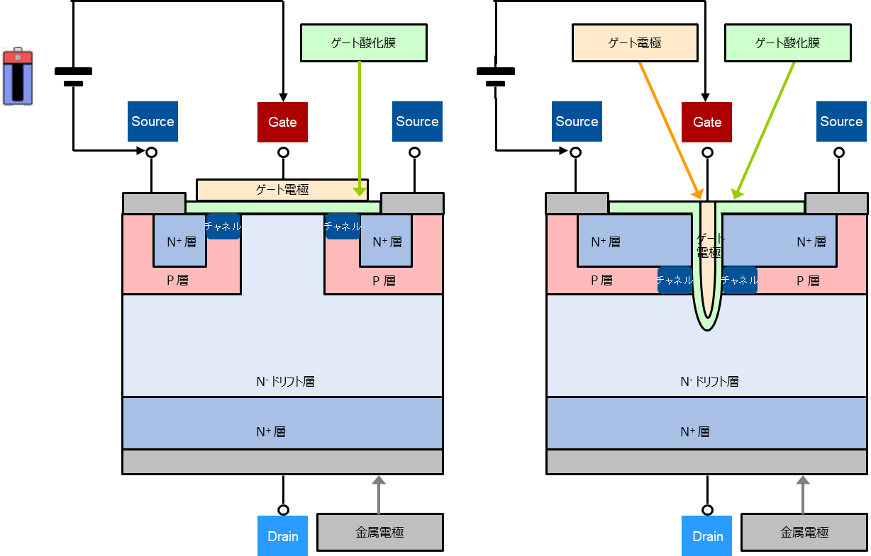
Advantages: The planar structure allows the gate to be made on a flat surface with few irregularities, which allows it to maintain stable characteristics and is suitable for low-capacity, high-speed SWITCHES. When the drain-source voltage of MOS FETS is medium to high (VDSS of approximately 250V or higher), many products use the vertical planar structure.
-
Problem: On the other hand, with planar types, the channel is formed horizontally on the surface of the wafer, so the channel length limits the cell size. Since the cell size cannot be reduced below the channel length, each cell size becomes larger.
In addition, a depletion layer forms between the P layer and N- drift layer, narrowing the path through which the drain current ID passes. This depletion layer limits the drain current, similar to the principle of a JFET, and when the planar structure is miniaturized to reduce the on-resistance Rds(on), the JFET resistance increases, making it difficult to miniaturize the cell.
Furthermore, in the case of a planar structure MOS FETS, the drift layer must be thicker to increase the breakdown voltage, which increases the on-resistance Rds(on).
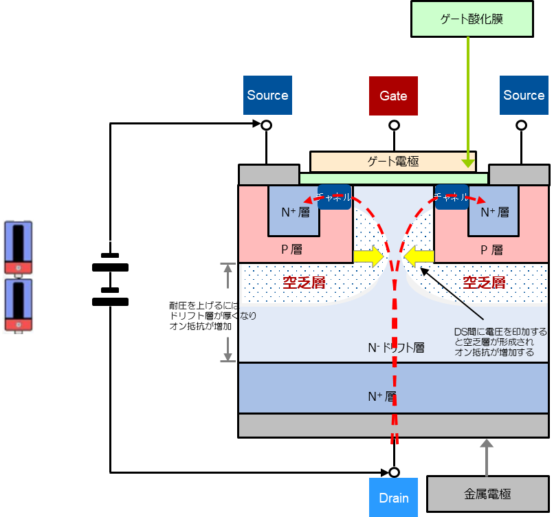
Advantages and disadvantages of planar type
Trench type
-
Advantages: In the trench structure, the channel is formed vertically, which allows for cell miniaturization. As a result, many cells can be arranged side by side, which reduces the on-resistance Rds(on) and allows for more current to flow. In addition, the absence of a JFET in the structure makes it suitable for miniaturization.
-
Problems: On the other hand, trench types have a structure in which a groove (trench) is dug from the surface of the wafer and the gate electrode is buried, which makes the manufacturing process more difficult than with planar types and makes yields more likely to deteriorate.Furthermore, because trench types are not suitable for high voltage resistance, most products with a vertical planar structure are used when the drain-source voltage resistance of MOS FETS is medium to high (VDSS of approximately 250V or more).
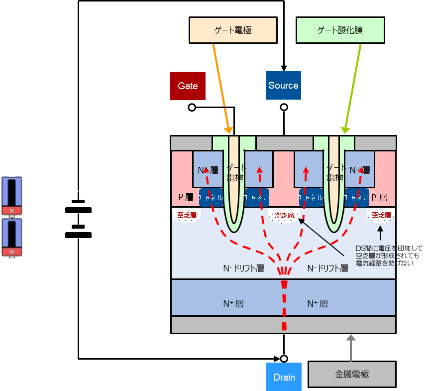
Advantages and disadvantages of trench type
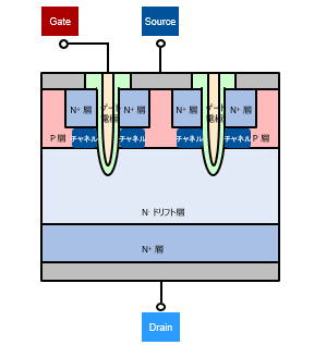
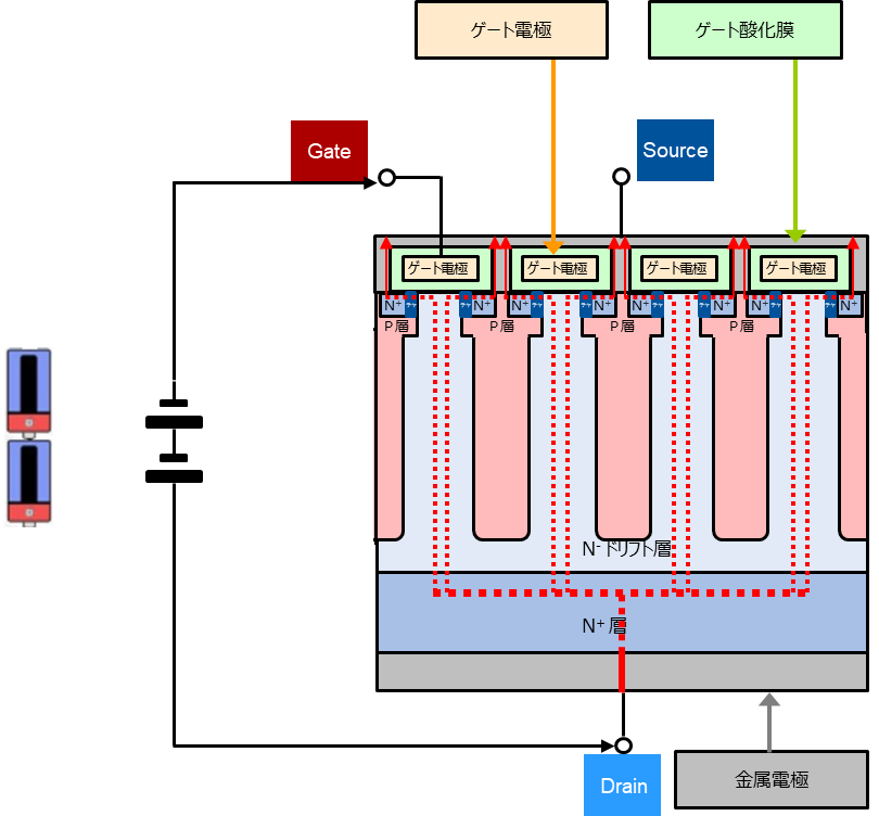
Differences between high-voltage planar and superjunction types
Similarly, we will look at the differences between planar and superjunction types.
In a planar structure, TRANSISTORS are configured flat, so increasing the breakdown voltage creates a problem in that the drift layer becomes thicker and on-resistance Rds(on) increases.The superjunction structure has multiple vertical pn junctions arranged side by side, which reduces on-resistance Rds(on) and gate charge Qg while maintaining the breakdown voltage.
*The superjunction structure was developed to overcome the limitations of the planar structure.
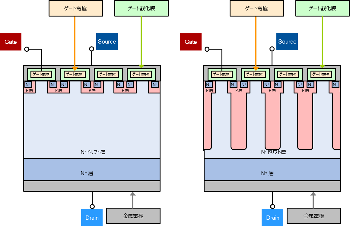
Comparison of the basic structures of high-voltage planar and superjunction types 1
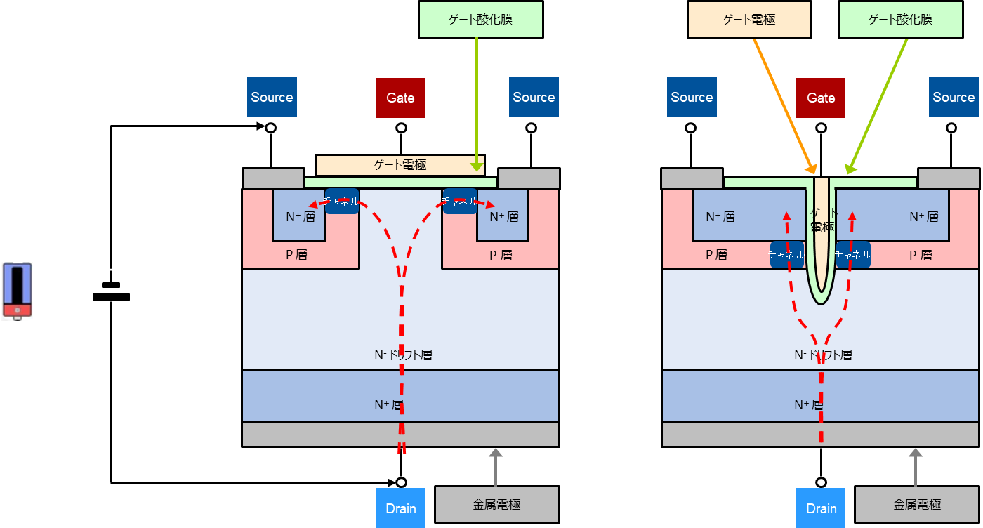
In high-voltage planar types, the depletion layer expands in response to the voltage applied between the source and drain, and this is a factor in increasing the breakdown voltage. The expansion of the depletion layer results in its thickness, so as the breakdown voltage of MOS FETS is increased, the drift layer must be made thicker, making it difficult to lower the on-resistance Rds(on). On-resistance Rds(on) can also be reduced by increasing the impurity concentration in the drift layer, but increasing the impurity concentration thins the depletion layer, making it impossible to ensure sufficient breakdown voltage. Therefore, the higher the breakdown voltage, the greater the resistance of the drift layer, and the greater the on-resistance Rds(on).
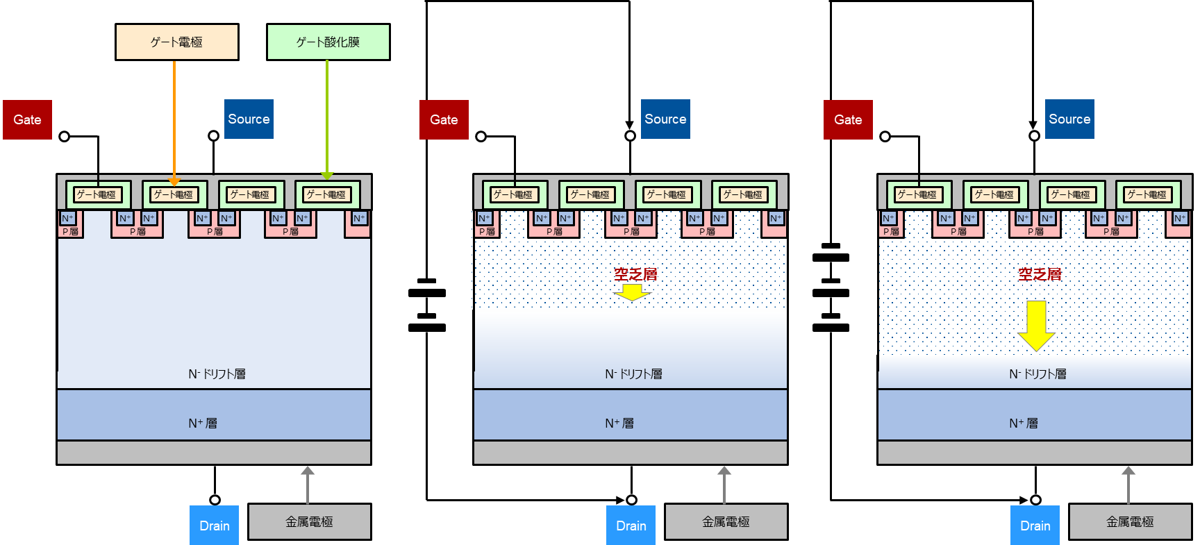
Comparison of the basic structures of high-voltage planar and superjunction types 2
On the other hand, in the superjunction structure, when a high voltage is applied between the source and drain in the off state (gate voltage is zero), the depletion layer spreads laterally from the pn junction between the n-type column and the p-type column, and eventually the entire drift layer becomes completely depleted (electric charge disappears), ensuring high breakdown voltage.
In addition, the impurity concentration in the drift layer can be increased by about five times, making it possible to reduce the on-resistance Rds(on) even when the breakdown voltage is increased.
Comparison of the basic structures of high-voltage planar and superjunction types 3
Superjunction type
-
Advantages: In the superjunction structure, although the channel is formed laterally, it is possible to miniaturize the cells. As a result, the cells can be arranged at high density, and the on-resistance Rds(on) can be significantly reduced. Also, as mentioned above, by increasing the impurity concentration, it is possible to reduce the on-resistance Rds(on) while increasing the breakdown voltage, which enables the transmission of large currents.
-
Problems: However, although the on-resistance Rds(on) is low, the output capacitance Coss and parasitic capacitance tend to be relatively large, which can increase the energy (charge/discharge loss) during SWITCHES. Also, because the body DIODES /recovery characteristics differ from conventional structures, it can be difficult to achieve soft recovery, so care must be taken when designing the circuit.
Advantages and disadvantages of the superjunction type
Advantages of ST's MOS FETS
Here we will explain the benefits of considering ST's MOS FETS (MOS FETS product lineup/long-term supply guarantee).
1. ST's MOS FETS products have a full lineup including planar type, trench type, and SJ type.
Over the years, SILICONE MOS FETS and IGBTS have been improved to replace MOS FETS planar structure with higher performance trench and superjunction structures, a natural progression to meet market needs for increased power density and energy savings.
ST's MOS FETS products have also continued to reduce on-resistance Rds(on), improve switching characteristics, and suppress product variation with each generation, from the F1 series to the latest F9 series in the low-voltage range, and from the SWITCHES series with a superjunction structure to the M9 series in the high-voltage range.
This offers the significant benefit of being able to select the optimal MOS FETS for your voltage range, structure, and application from within the same manufacturer. From the initial design stage through mass production and even to the rollout of next-generation models, the ability to smoothly transition from one generation to the next without making major changes to the device structure offers significant value in terms of effective use of circuit assets and reduced redesign man-hours.
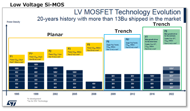
Low-Voltage SILICONE MOS FETS Lineup
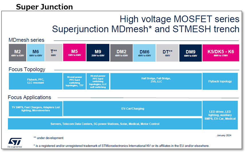
Super junction type lineup
2. Long-term supply guarantee
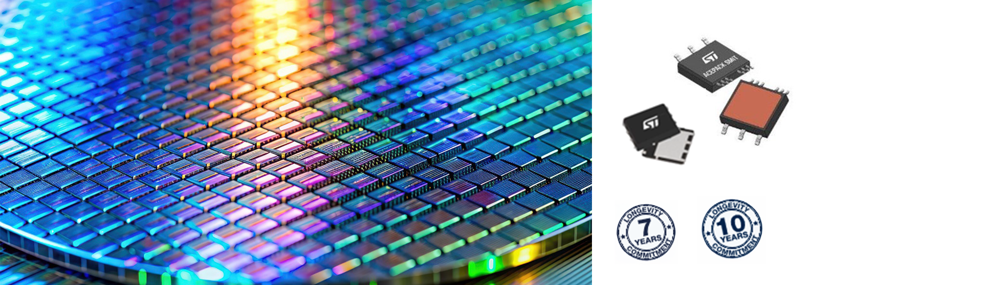
The majority of ST's STPOWER SiC MOS FETS, low-voltage/high-voltage SILICONE MOS FETS, IGBTS, and intelligent power modules (IPMs) are certified and published as products covered by ST's 10-year longevity guarantee program.
Commitment to long-term supply: The following is a Japanese translation of the content from ST's website.

Logo indicating long-term supply guarantee
STMicroelectronics commits to a minimum 10-year lifespan for products covered by the program.
If a product you are interested in is not currently covered by the program, please Inquiry your local sales office. The 10-year supply commitment includes the notice period outlined in the standard STMicroelectronics End of Supply Notice Policy (PTN). In the event of a significant production reduction, technology or manufacturing change, STMicroelectronics may elect to switch to a comparable product, different technology, or different manufacturing facility and will notify customers of this using the standard STMicroelectronics Product/Process Change Policy (PCN).
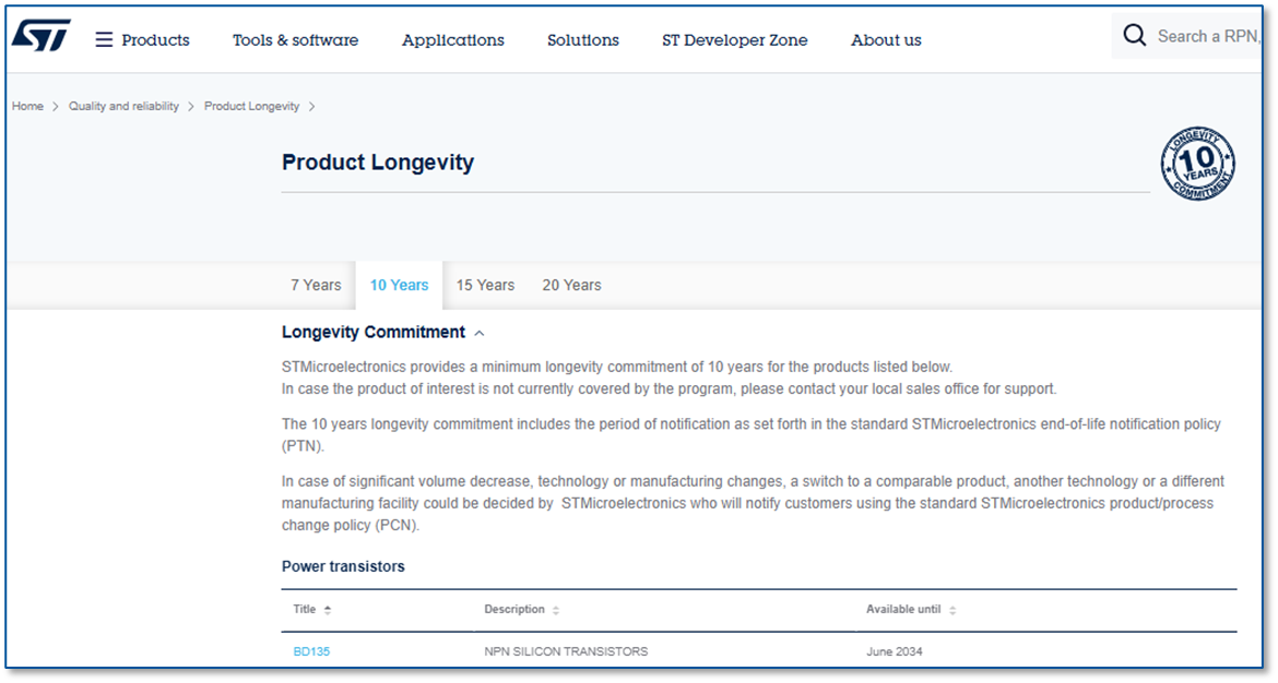
ST's long-term supply guarantee page
Summary
MOS FETS vary greatly in on-resistance, SWITCHES loss, EMI, thermal characteristics, and even cost structure depending on the device structure.
Accurately understanding the differences in the structure and operating principles of various FETs is key to quickly selecting the device that is best suited to your circuit conditions and design goals.
The basic selection guidelines for each application are as follows:
- When the top priority is low on-resistance Rds(on) and high efficiency at low voltage (for example, up to 100V) → trench type is the first choice
- When high voltage resistance (several hundred to thousands of volts) and low loss are essential → Superjunction type is the best choice
- If reliability, avalanche resistance, ease of use, and low cost are important → Planar type is suitable
Note that SWITCHES speed evaluation is not determined solely by the structure, but the final loss is determined by a combination of on-resistance Rds(on), gate charge Qg/Qgd, output capacitance Coss, and DIODES recovery characteristics. Therefore, it is necessary to comprehensively compare and evaluate multiple indicators, rather than just a single indicator on the datasheet.
The commonly used formula for FOM (figure of merit) is as follows:
- On-resistance Rds (on) × gate capacitance Cg
- On-resistance Rds (on) × gate charge Qg
Both formulas make it possible to easily compare SWITCHES performance of MOS FETS.
If you have any concerns about selecting or replacing MOS FETS, please feel free Inquiry us.
Related Info
- Power MOS FETS in general: Power MOS FETS- STMicroelectronics
- Trench MOS FETS: N-channel MOS FETS (> 30V - 200V) - STMicroelectronics
- Super-Junction FETs: Super-Junction MOS FETS (200V - 700V) - STMicroelectronics
- Longevity Guarantee (7 Years): Longevity Guarantee - STMicroelectronics
- Longevity Guarantee (10 Years) Longevity Guarantee - STMicroelectronics