In high-power SWITCHES circuits such as automotive traction INVERTERS, DIODES are essential for the charge pump circuits and DESAT detection circuits in GATE DRIVER. However, reverse recovery losses that are not noticeable in average power consumption can lurk in these circuits and lead to sudden breakdowns after mass production. This article explains the reverse recovery operating principle and loss mechanism of DIODES, as well as design considerations and evaluation methods, and provides indicators that can help prevent problems before they occur.
"Invisible" risks that occur in high-power SWITCHES circuits
Widely used essential circuits in high-power INVERTERS are DESAT circuits, which protect SWITCHES elements from abnormal losses, and charge pump circuits, which generate the gate voltage required for N-channel MOS FETS.
Both use DIODES, but because a large instantaneous current flows due to reverse recovery operation, there is a risk of destruction due to the following reasons that are difficult to determine using average power consumption indicators.
- Because the average power consumption is small, even if the reverse recovery loss is abnormal, it does not affect the efficiency or input current of INVERTERS circuit.
- Reverse recovery characteristics are often not specified in specifications and are easily overlooked during the design stage.
- There is a persistent misconception that "there is no problem if DIODES is used for SWITCHES purposes"
For this reason, it is important to correctly understand the principles behind DIODES reverse recovery loss and the basis for confirming safety.
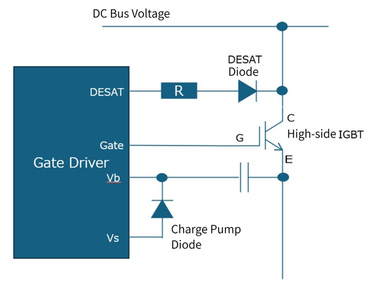
Example circuit diagram including DESAT and charge pump
Reverse recovery principle and loss mechanism
While DIODES is conducting in the forward direction (ton in the diagram below), carriers accumulate inside the device. When a reverse voltage (red waveform in the diagram below) is applied to DIODES to block the current, a reverse recovery current (blue waveform in the diagram below) flows to remove the charge that had accumulated across DIODES while it was conducting. This phenomenon is called reverse recovery operation.

DIODES reverse recovery operation
With high-speed SWITCHES, reverse recovery loss occurs as the reverse voltage rises before the reverse recovery operation is complete, and the reverse voltage x reverse recovery current overlaps. Reverse recovery characteristics are given as the reverse recovery time trr and the reverse recovery current Irr, but it is important not to confuse them with the voltage rise and fall values as they are specifications related to current and charge.
Specific situations where reverse recovery becomes a problem in GATE DRIVER
With DESAT detection, losses concentrate in DIODES in response to sudden voltage changes. With charge pumps, reverse recovery occurs repeatedly depending on SWITCHES frequency, and even though the average power consumption is small, instantaneous peaks can trigger thermal stress or overcurrent. These are all typical examples of how "invisible" losses can threaten long-term reliability.
Reverse recovery loss estimation
Reverse recovery characteristics are expressed in various ways depending on DIODES manufacturer, such as reverse recovery charge Qrr, reverse recovery time trr, or reverse recovery current Irr. The maximum value of loss based on these relationship formulas is given by the simplified formula below, so it is recommended to use this to find the initial value of DIODES loss.
- Reverse recovery loss [W] = Maximum voltage [V] x Reverse recovery charge [C] x SWITCHES frequency [Hz]
- Reverse recovery charge [C] = Reverse recovery current [A] x Reverse recovery time [s]
Calculation example
INVERTERS circuit: Maximum bus voltage Vmax = 600V, SWITCHES frequency f = 20kHz
DIODES: trr = 150ns, Irr = 3A
Considering the above, the reverse recovery loss can be calculated as follows, resulting in 5.4 W.
- Reverse recovery charge Qrr = Irr × trr = 3A × 150ns = 450nC
- Energy loss per cycle: E = Vmax × Qrr = 600V × 450nC = 0.27mJ
- Average reverse recovery loss Prr = 0.27mJ × 20kHz = 5.4W
This "average of 5.4 W" is by no means small for a single DIODES. Depending on the heat capacity, heat dissipation conditions, and waveform peak shape, instantaneous stress can cause destruction.
The importance of DIODES selection
Fast recovery diodes (FRDs) and SiC DIODES are likely candidates for use in charge pumps and DESAT applications. Because general-purpose rectifier DIODES are not designed for SWITCHES applications, their reverse recovery specifications are often not fully disclosed, making it difficult to ensure a safety margin at the design stage.
Even with FRDs, reverse recovery times may not be sufficient depending on the application. It is important to select a product with a small Qrr and mild temperature and di/dt dependency, and to carry out a series of tests to confirm the waveform under actual conditions. SiC has an extremely small Qrr due to a structure that does not involve minority carrier accumulation, which is advantageous for reducing reverse recovery losses during high-speed SWITCHES, but its high distribution price remains a drawback.
The table below lists different types of DIODES with similar specifications so that you can see the differences in their characteristics (this does not mean that these are suitable for DESAT or charge pumps). As you can see, the Qrr value varies greatly depending on the type of DIODES. We have also listed Cj for reference, but please note that Cj is the capacitance of the static junction only, and is a different specification from the Qrr of the entire DIODES.
| Model number | DIODES Type | Rated current [A] | Breakdown voltage [V] | Reverse recovery time trr | Reverse recovery charge Qrr | Junction capacitance Cj | Forward voltage VF [V] |
|---|---|---|---|---|---|---|---|
| 1Nxxxx | General-purpose | 3 | 1000 | Approximately 2-3 μs | Hundreds of nC to μC | 500 pF | 1.1 |
| Exxx | FRD | 3 | 600 | 35 ns | Approximately 30-50 nC | 60 pF | 1.7 |
| C3Dxxxxxx | SiC | 6 | 600 | <20 ns | ~5 nC | 30 pF | 1.35 |
Comparison table of similar sized DIODES
How to proceed with evaluation and confirmation
Because reverse recovery characteristics vary slightly depending on conditions, we observe the reverse recovery waveform using a high-speed current probe and differential voltage probe on an oscilloscope with a bandwidth of over 200 MHz. We align the load conditions and SWITCHES frequency of the target GATE DRIVER board with those for actual use and capture the overlap of voltage and current in the trr region. Temperature measurement is necessary not only at the maximum temperature, but also at the minimum temperature, as there is a possibility that the instantaneous rated current withstand capacity may be exceeded. Furthermore, we change SWITCHES di/dt to estimate Prr under worst-case conditions and evaluate the thermal design margin. This allows us to quickly identify risks arising from the actual waveform that cannot be determined from specifications alone.
Summary
As explained in this article, reverse recovery operation can cause a momentary high power to concentrate in DIODES. This can be a common pitfall, as it's easy to miss if you only look at average losses and won't be noticed unless you observe the current waveform. For GATE DRIVER applications, we recommend incorporating appropriate model selection and evaluation based on actual waveforms into the standard flow, and adding Qrr and trr check items to the design checklist. This is a surefire way to prevent defects after mass production. Please feel free Inquiry if you have any questions.
Inquiry
Related Product Information

LITIX™ Automotive LED DRIVER ICHighly efficient and reliable LED DRIVER IC optimized for automotive lighting. Supports a wide range of applications, from animation lamps to matrix headlamps.
LITIX™ is a family of automotive LED DRIVER ICs that features constant current control and diagnostic and protection functions, making it highly efficient, reliable, and compatible with a wide range of lighting control applications.
- Infineon Technologies AG
- NEXT Mobility

Introduction to NXP's Automotive Millimeter-Wave Radar Products
This article provides an overview of automotive millimeter-wave radar, a key sensor in advanced driver-assistance systems (ADAS), and introduces NXP’s leading radar product family driving the market.
- NXP Semiconductors NV
- NEXT Mobility
- ICT and Industrial
- Smart Factories and Robotics
GMSL High-Speed Transmission Technology for Automotive Applications
This explains the high-speed transmission technology GMSL.
- Analog Devices, Inc.
- NEXT Mobility
MAX77726/MAX77727: 22V, 3A synchronous step-down converter (with ultrasonic mode)
The MAX77726/MAX77727 are high-efficiency step-down converters for ultra-low power devices. They support ultrasonic mode and I2C control.
- Analog Devices, Inc.
- ICT and Industrial

CoolSiC™ MOS FETS "CoolSiC™ MOS FETS supports next-generation electrification" High efficiency, high voltage resistance, and high reliability. SiC power MOS FETS ideal for EVs, renewable energy, and industrial equipment.
Infineon's CoolSiC™ MOS FETS offer high voltage resistance, low loss, and high temperature operation, contributing to improved efficiency and reliability of EV and industrial POWER SUPPLIES.
- Infineon Technologies AG
- NEXT Mobility
- ICT and Industrial

Gate Driver Infineon's gate drivers deliver high efficiency and reliability, accelerating the next generation of power electronics.
Infineon's gate drivers control high-power devices with high precision and safety, and their high insulation voltage and diverse functions support reliability in automotive and industrial applications.
- Infineon Technologies AG
- NEXT Mobility
- ICT and Industrial