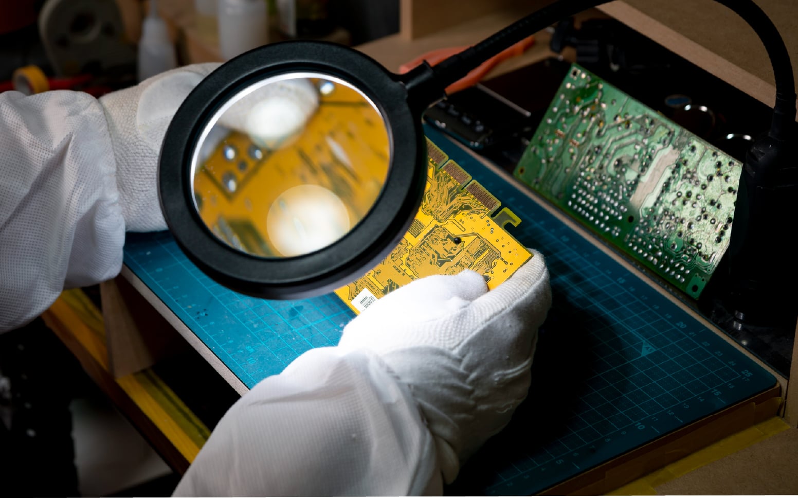
What is Failure Analysis?
Semiconductor Failure Physical Analysis is the process of investigating and identifying the root cause of
semiconductor device failures from a physical perspective.
Failure analysis is essential for
understanding failure mechanisms and improving device reliability.
At NEXTY Electronics, we follow
standard failure analysis methods commonly used by semiconductor manufacturers to determine the cause of
failures.
NEXTY Electronics Failure Analysis Services
Among the various types of semiconductor device failures, those caused by EOS (Electrical Overstress) and
ESD (Electrostatic Discharge) are frequently observed.
Each device manufacturer specifies an Absolute
Maximum Rating in the datasheet, which represents the maximum voltage or current that must never be
exceeded, even momentarily. When these limits are surpassed, the device may be damaged, resulting in
EOS/ESD failures.
Because EOS/ESD failures occur under stress conditions outside the manufacturer’s warranty, analysis
requests are often declined by the manufacturer.
In such cases, NEXTY Electronics performs EOS/ESD failure analysis using standard methods and
equipment employed by semiconductor manufacturers.
In addition to EOS/ESD failures, we also infer possible root causes based on findings obtained
through failure analysis. (See the list of analysis items below.)
Failure Analysis Items
| Analysis Item | What Can Be Identified |
|---|---|
| Visual Inspection | Scratches (depth), cracks, corrosion, discoloration, burn marks, foreign material adhesion |
| X-ray Inspection | Wire breakage, wire edge touch, foreign material, frame deformation, burn marks |
| VI Characteristic Measurement | Short between terminals, open circuit, leakage |
| SAT Inspection | delamination at the chip interface, delamination at the inner lead interface, delamination at the die pad interface, delamination at the die‑attach interface , voids |
| Chip Surface Observation | Burn marks, corrosion, disconnection, foreign material |
| OBIRCH Observation *Backside observation available | Identification of burn damage not exposed on the chip surface *For backside observation, mold resin, die pad, and die attach material are removed, and OBIRCH observation is performed from the backside of the Si chip. For details, please refer to backside polishing for OBIRCH observation. |
Failure Analysis Process
Visual Inspection
Inspect Package Appearance for Abnormalities
After receiving the sample, we first check for external abnormalities such as
scratches, cracks, discoloration, or foreign material contamination.
Package dimension
measurement is also available.
Equipment: Microscope KEYENCE VHX-5000
-

Package surface inspection
-

Package dimensional measurement
-
Foreign material between leads
Equipment: Laser Microscope KEYENCE VK-X200
We support surface profile measurement and also roughness measurement using a laser
microscope.
1.Bulging detected at the center of the package and measured with the laser
microscope.
2.The bulge on the package visualized as a 3D image, confirming the deformation at the
center.

▼
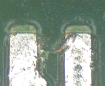
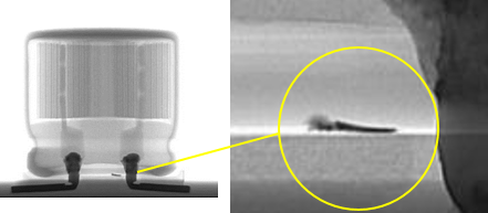
X-ray Inspection
Observation of internal package abnormalities
X-ray inspection enables non-destructive confirmation of internal defects. This method allows detection of issues such as wire sweep, burning, wire breakage, wire cracks, edge touch, and foreign material contamination—defects that cannot be seen from the outside of the package.
Equipment: X-ray System Nordson DAGE QUADRA5
-

Chip-and-wire burn damage
(EOS-induced damage) -

Wire sweep: Wire contacting adjacent wire
-

Wire crack: Crack occurring at the neck, causing disconnection
-

Wire Deformation: Wire is deformed and touches the chip edge.
-
Foreign Object Contamination: Metallic fragment observed directly beneath the aluminum electrolytic capacitor.

▼
Electrical Characteristic Measurements
VI Characteristic Measurement/Resistance Measurement/Capacitance Measurement/Inductance Measurement
In VI characteristic measurement, a source meter is used to measure the voltage-current characteristics between terminals. This allows for the identification of leakage, short circuits, and open circuits.
Equipment: Source Meter KEITHLEY 2601B
-
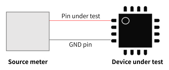
VI Characteristic Measurement Diagram:Voltage applied to the target pin / Current measurement
-
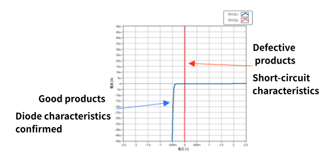
VI characteristic measurement waveform results:For good products, diode characteristics can be confirmed, whereas defective products exhibit short-circuit characteristics, indicating failure.
-

WAYNE KERR/3260B
-

Example: Capacitor Capacitance Measurement Result
LCR Meter: For resistors, capacitors, and inductors, an LCR meter is used to measure resistance, capacitance, and inductance, and to check for deviations from standard values.

▼
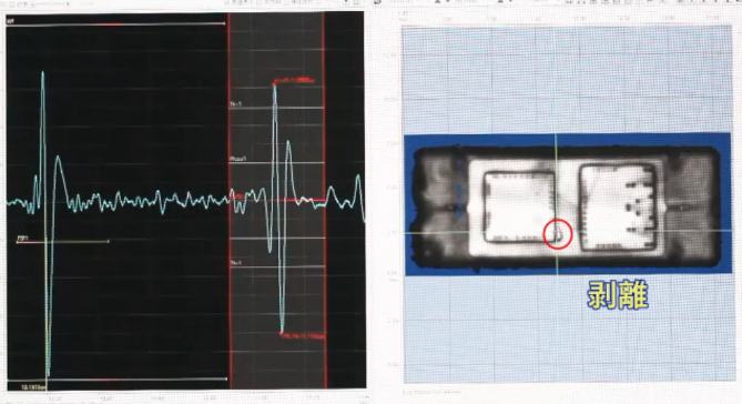
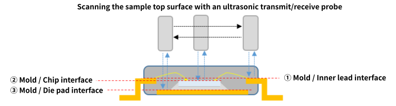
SAT (Scanning Acoustic Tomography)
Observation of delamination inside the package
Reflection Method
When the sample to be analyzed is placed in water and exposed to ultrasonic waves,
reflected waves return from the sample.
The magnitude of the reflected wave depends on the
difference in acoustic impedance (the ease with which sound propagates) between materials—the
greater the difference, the stronger the reflection.
Since the sample consists of multiple materials, differences in acoustic impedance occur at
the interfaces between these materials.
The reflection method utilizes this property to observe delamination at material interfaces.
Equipment: INSIGHT / INSIGHT-300 Available probes: 25 MHz / 50 MHz / 75 MHz
Video: During equipment operation
Example: Delamination Observation Using SAT
Imaging of internal package interfaces (die pad interface)
In a typical IC package structure, the following interfaces are observed using the reflection
method:
①Mold / Lead Frame Interface②Mold / Chip Interface③Mold / Die Pad Interface
-
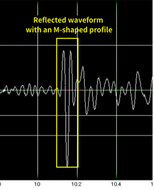
Reflection waveform:No delamination: M-shaped
-
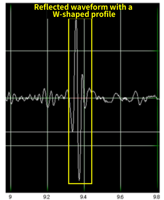
Reflection waveform:With delamination: W-shaped
Observation between chip and die pad (to check for delamination of die attach material) is performed using the transmission method.
Transmission Method
In the transmission method, ultrasonic waves passing through the material are
detected to observe the presence of delamination or voids.
If there is an air layer such as
delamination or voids, the density of the medium decreases significantly, causing the transmitted
ultrasonic wave to attenuate greatly. This appears as a black area in the image.
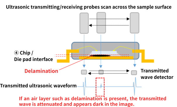
Transmission Image Between Chip and Die Pad:
-
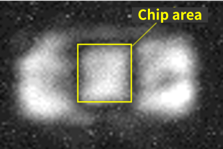
No delamination: No black shadow in chip area
-
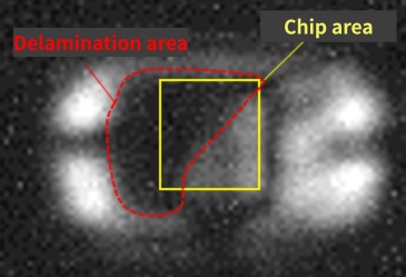
With delamination: Black shadow extends to chip and die pad areas

▼
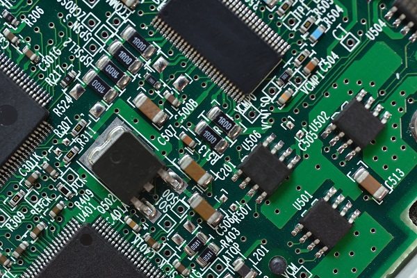
Package Opening & Chip Surface Observation
Resin is dissolved using chemicals.
First, the mold resin is thinned by laser processing, then the package resin is
dissolved with chemicals to expose the chip surface.
The exposed chip surface is observed using
a microscope or SEM to check for abnormalities such as burn marks, passivation cracks, wiring
corrosion, and bonding shape defects.
QFP Cu Wire Package Opening
Note: Cu/Ag wires dissolve with conventional chemical
treatment alone. To observe wires, unnecessary resin is removed by laser processing beforehand,
and the contact time between chemicals and wires is minimized to reduce wire damage during
opening.
-
Laser Opening
-
Chemical Opening
-

Chip burn-out caused by EOS (Electrical Overstress)
-
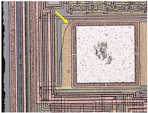
Passivation layer cracks
Opening of a quartz crystal oscillator
Mechanical opening of metal packages in addition
to mold resin
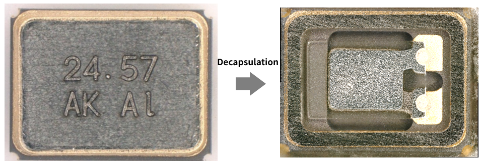
Metal packages are thinned by polishing for opening


▼
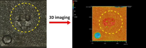
IR-OBIRCH Analysis
Identifying Defective Areas on the Chip
Electrical abnormalities such as short circuits, leakage, or high resistance may be
confirmed, but no abnormalities are visible on the chip surface. In such cases, defects may exist in
the lower layers beneath the surface.
IR-OBIRCH scans the chip with a 1.3 μm wavelength laser
while applying a constant voltage.
Defective areas exhibit significant resistance changes due to laser heating compared to normal
areas.
These resistance changes are detected as current values, and by synchronizing laser scanning
with current measurements, defective areas are identified.
Equipment: IR-OBIRCH System – HAMAMATSU PHOTONICS PHEMOS-1000
-
During OBIRCH Operation:
Defect localization using IR-OBIRCH: Observation from the backside of the Si substrate
Equipment: Backside Polisher – ULTRA TEC
When the top metal wiring layer is too thick or multilayered, making it difficult for
laser heat to reach lower wiring or circuit elements, backside polishing is used to expose the Si
substrate.
Laser heating and observation are then performed from the backside, as 1.3 μm wavelength light
can penetrate Si.
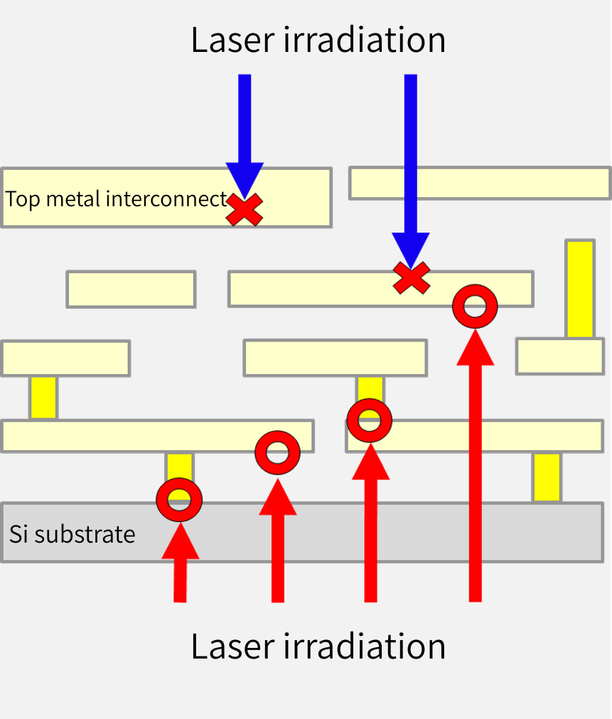
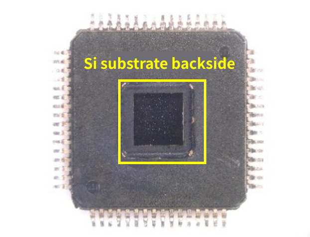
After Backside Polishing – Package
From the backside of the package, the die pad is thinned to expose the backside of the Si substrate.

▼
Report Submission
Request Process
Inquiries and quotations are free of charge.
Our services are available for devices other than those
handled by NEXTY Electronics.
Please feel free to contact us if you are interested.
1. Inquiry
Submit your request via the inquiry form, including details such as sample information, quantity,
budget, and desired delivery date.
If you have related documents, please send them together. (Sample information and budget can be provided
within the range you are comfortable sharing.)
2. Response and Quotation
A NEXTY Electronics representative will review your inquiry and confirm details during a hearing
session.
We will check the analysis content, feasibility, and any additional requirements, then
provide an estimate and delivery schedule.
After reviewing the analysis details, quotation, and
delivery date, if you decide to proceed, we will send a formal quotation.
3.Order Placement and Shipment of Analysis Samples
Please send us your official order form. Upon receipt, we will begin the analysis process.
The shipping address for samples will be provided by NEXTY Electronics.
4. Analysis Execution
We will perform the requested analysis.
If you require interim results, we can provide a mid-term
report upon request.
Examples:
Report before moving from non-destructive to destructive analysis
Early results for large-volume analysis
5.Report Delivery
The analysis results will be compiled into a report and sent to you.
If you have any questions or
require clarification, please feel free to contact us.
6. Payment and Sample Return
After acceptance, NEXTY Electronics will return the samples along with the invoice, receipt, and
delivery note.
Please proceed with payment accordingly.
Contact Us
We accept consultations, questions, and quotation requests via the button below.
Our services are
available for devices other than those handled by NEXTY Electronics.
For quotation requests, including the following information will help us respond smoothly:
Even if the information is not listed, please feel free to contact us. Once confirmed, a representative
will get back to you.
Required Information for Quotation Request:
Request details:
Sample information:
Quantity:
Budget:
Desired delivery date:
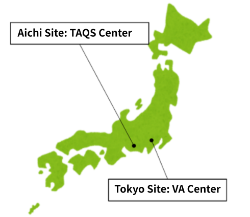
Our Service Locations
Aichi OfficeTAQS(Toyotsu Automotive Quality Support Center)
| Location | Toyotsu Logistics Services Bldg 4Fl. 1-3 Oonawa, Ozaki-cho, Anjyo, Aichi, 446-0004, Japan |
|---|---|
| Supported Services | Failure analysis, Good Product Analysis, Reliability Testing: Accelerated Testing, Cross-section analysis |

NEXTY Electronics’ VA Center Division operates two locations to provide quality and analysis services
to our customers: the VAC (Value Adding Center) in Tokyo and the TAQS (Toyotsu Automotive Quality
Support Center) in Aichi Prefecture.
We will respond from the location that can deliver the services you require. If you have any
requests, please contact us using the inquiry button below.
Key Points of Our Quality and Analysis Service Locations
At NEXTY Electronics’ VA Center Division, we provide reliable quality and analysis services you can rely on, supported by a comprehensive framework as outlined below.
- Building Facilities
Robust Earthquake-resistant Structure
- Security
Surveillance Camera Monitoring, Access Control System
- Work Environment
Temperature and Humidity Control Anti-static Measures
View More Quality & Analysis Services
-
Failure Analysis
Initial Diagnostics, One-Stop Support

-
Good Product Analysis
Early Identification of Potential Product Risks

-
Reliability Testing: Accelerated Testing

-
Reliability Testing: Evaluation Testing

-
Cross-section analysis
Non-Visible Internal Analysis

-
Reverse Engineering

-
Optical Characterization of LEDs

-
ROM Writing Service

-
Screening Inspection (Visual and X-ray)

-
Automotive Ethernet Testing Services

-
Analysis of the 10 Substances Regulated under the RoHS Directive

-
-
Quality and Analysis Support by NEXTY Electronics